Deposition Repair Apparatus And Methods

a technology of deposition and repair apparatus, which is applied in the manufacture of electric discharge tubes/lamps, lighting and heating apparatus, instruments, etc., can solve the problems of mask problems, unavoidable defects, and affecting the electrical and/or optical performance of the final lcd produ

Active Publication Date: 2008-06-12
NAVY USA AS REPRESENTED BY THE SEC OF THE THE +1
View PDF25 Cites 40 Cited by
  • Summary
  • Abstract
  • Description
  • Claims
  • Application Information

AI Technical Summary

Benefits of technology

[0034]In one embodiment, the apparatus further includes, in part, an auto-focus sensor having an optical path coaxial with the optical path of the camera, the first and second lenses when selectively used in operation, and the laser beam. The auto-focus sensor maintains the distance between the substrate and the first lens within the predefined range during the material removal operations. The auto-focus sensor further maintains the distance between the ribbon and the second lens within the predefined range during the transfer of the rheological compound. In some embodiments, the auto focus sensor is a tracking auto focus sensor maintaining the distance between the ribbon and the substrate within the predefined range as the ribbon is moved relative to the substrate.

Problems solved by technology

During each of these stages and at various steps within each stage, many production defects may occur that may affect the electrical and / or optical performance of the final LCD product.
Other defects include mask problems, over or under etching, etc.
Even though the TFT deposition processes are tightly controlled, defect occurrence is unavoidable.
This limits the product yield and adversely affects production costs.
Usually AOI and AC systems provide defect coordinates; they do not provide high resolution images required to classify defects as killer defects, reparable defects, or imperfections that do not affect TFT array performance (also known as process defects).
Compared to repairs requiring cutting such as shown in FIG. 2, repairs requiring correction of open paths such as shown in FIG. 3 are far more challenging, because new material must be introduced to correct such defects.
Currently, the LCVD process is slow and its associated tools are expensive, and FP production lines typically include a number of lower cost review / cutting repair tools, such as the ASx60 products manufactured by Photon Dynamics, Inc., and a separate LCVD tool dedicated for line open repairs. FIG. 19B illustrates the current typical flow of FP plates through the sequence of review / repair tools in a production line.
The LIFT method is not suitable for organic materials because it is a high temperature method.
Further, since high temperatures are achieved at the target material, ablation or sputtering of the target substrate itself may also occur, resulting in transfer of the target substrate material which reduces the integrity of the purity of the desired film material.
There have been reports that lines created by the LIFT process have poor uniformity, morphology, adhesion and resolution.
Since both LIFT and MELD require the vaporization and condensation of a metal film on the surface of a substrate, the functionality (i.e. electrical conductivity) of the resulting patterns is marginal since the material exhibits numerous discontinuities between adjacent voxels (or transferred 3-dimensional pixels).
However, shortcomings of this approach to achieve lines less than 10 micrometer in width include: (i) highly complex process dependencies (for example, ink temperature, ink viscosity, atomizer pressure and temperature, gas sheath flow), (ii) frequent clogging of delivery needle, (iii) mean of droplet distribution limited to approximately 5 micrometer, which limits line width minimum to approximately 7 micrometer, (iv) limited to materials having viscosities less than about 1000 cP; and (v) factors determining linewidth include mean of droplet distribution, ink viscosity, ink / substrate surface tension, temperature.
Though developments continue, inkjet technologies for very fine line widths have not yet been proven for production.
Many of the same limitations listed above for aerosol jet technology apply to the print-on-demand inkjet technologies.
However, the conditions for jetting behavior as described in the '015 patent requires relatively thick coatings (1 to 20 micrometers thick, and more specifically 5 to 10 micrometers in the cited example) on the transparent ribbon, which result in equally thick transferred features, far larger than the sub-micron thickness required in FP repair.
Except for LCVD, other ink-based DW techniques, for example, jetting, cannot routinely achieve uniform and continuous sub-micron line thicknesses.
In the case of an ink jet system, for example, too large a distance may result in too wide a line (spread of jet) while too close a distance may also result in too wide a line (splatter of the jet).
Additional limitations to achieving 5 micrometer wide lines with good edge roughness using ink / rheological materials include: (iv) material particle size in the ink or rheological material, for metals, typical metal particles sizes should be in tens of nanometers or less, (v) aperture size in delivery mechanisms, and (vi) beam size of the laser or energy source.
Duignan's apparatus cannot be applied to laser direct write methods using rheological materials for a number of reasons such as (a) Duignan does not accommodate the requirement for maintaining consistent rheological material properties over time, (b) Duingan does not provide for the requirement for post-processing for the purposes of driving away the carrier components within the rheological fluid, etc.

Method used


Image

  • Deposition Repair Apparatus And Methods
  • Deposition Repair Apparatus And Methods
  • Deposition Repair Apparatus And Methods

Examples


Embodiment Construction

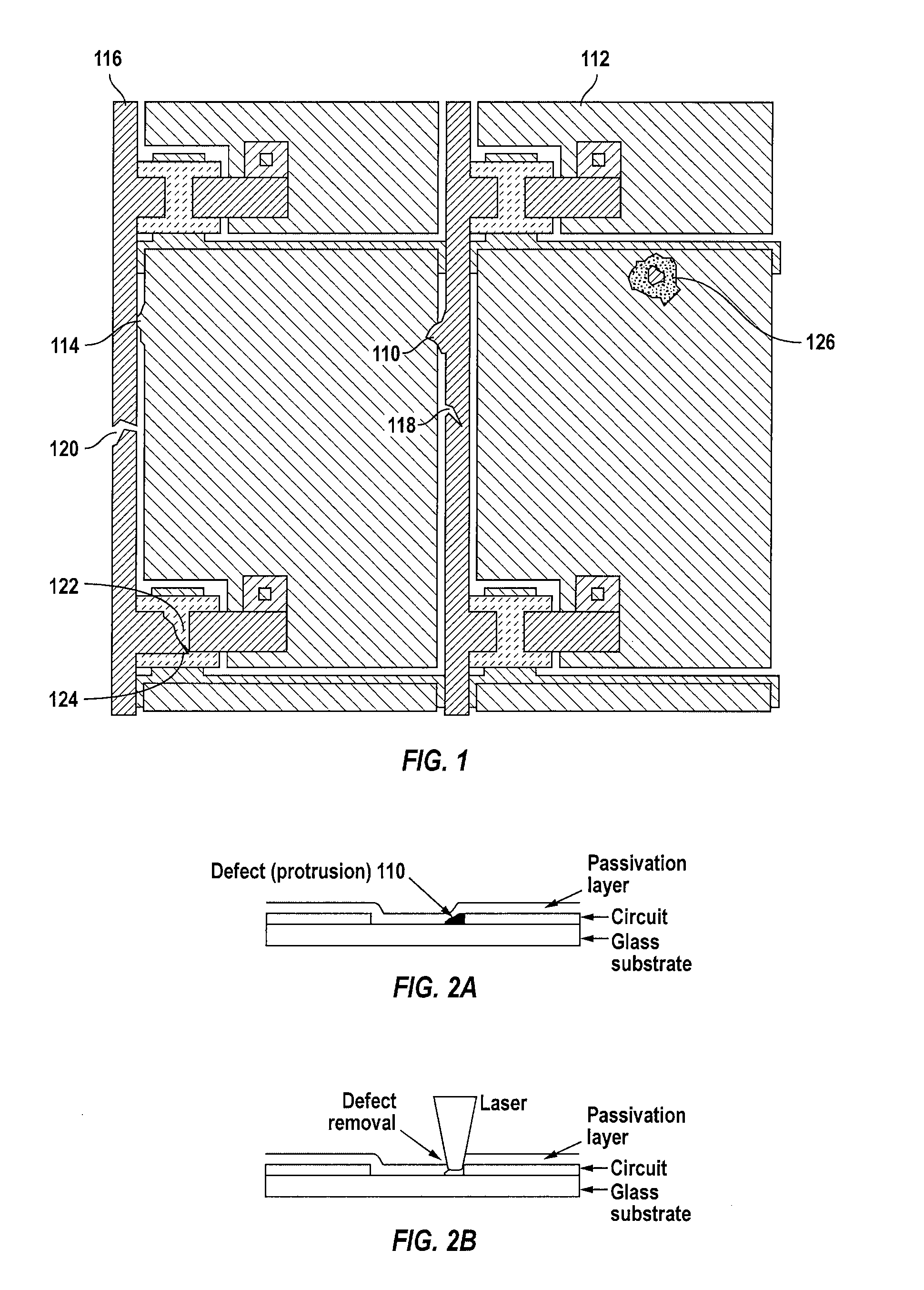
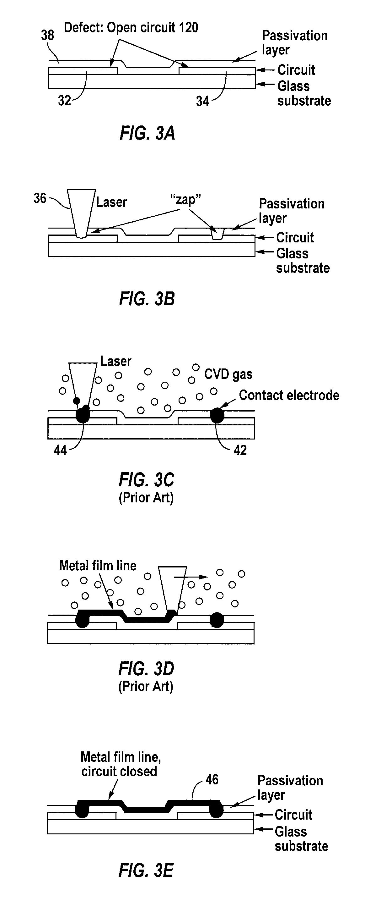
[0078]An apparatus, in accordance with one embodiment of the present invention, includes integrated review, material removal and material deposition functions. The apparatus performs the review, material removal and material deposition (transfer) operations along the same optical axis (path). The apparatus includes, in part, a camera, a pair of lenses, and one or more lasers. A first lens is used to focus the camera along the optical axis on a structure formed on the target substrate undergoing review. The first lens is also used to focus the laser beam on the structure to remove a material present thereon if the reviewed structure is identified as requiring material removal. The second lens is used to focus the laser beam on a ribbon to transfer a rheological compound from a recessed well formed in the ribbon to the structure if the reviewed structure is identified as requiring material deposition.

[0079]For purposes of the invention described herein, the terms “ink” and “rheologica...


PUM

PropertyMeasurementUnit
Depthaaaaaaaaaa
Depthaaaaaaaaaa
Fractionaaaaaaaaaa

Abstract

An apparatus includes integrated review, material removal and material deposition functions. The apparatus performs the review, material removal and material deposition operations along the same optical axis. The apparatus includes, in part, a camera, a pair of lenses, and one or more lasers. A first lens is used to focus the camera along the optical axis on a structure formed on the target substrate undergoing review. The first lens is also used to focus the laser beam on the structure to remove a material present thereon if the reviewed structure is identified as requiring material removal. The second lens is used to focus the laser beam on a ribbon to transfer a rheological compound from a recessed well formed in the ribbon to the structure if the reviewed structure is identified as requiring material deposition

Description

CROSS-REFERENCES TO RELATED APPLICATIONS[0001]The present application claims benefit under 35 USC 119(e) of U.S. provisional application No. 60 / 747,158, filed May 12, 2006, entitled “Line Open Repair Apparatus and Method”, the content of which is incorporated herein by reference in its entirety.BACKGROUND OF THE INVENTION[0002]The present invention relates generally to the non-contact repair of microelectronic circuits and in particular, to the repair of flat panel displays, such as active matrix liquid crystal display panels.[0003]During the manufacturing of liquid crystal (LC) displays, large clear plates of thin glass are used as a substrate for the deposition of thin film transistor (TFT) arrays. Usually, several independent TFT arrays are contained within one glass substrate plate and are often referred to as TFT panels. Alternatively, an active matrix LCD, or AMLCD, covers the class of displays utilizing a transistor or diode at every subpixel, and therefore encompasses TFT de...

Claims


Application Information

Patent Timeline
IPC IPC(8): H01L21/00H01J9/50
CPCB23K26/0003B23K26/046G02F1/136259B23K26/0613B23K26/048B23K26/351G02F1/13G02F1/1337F21S4/00
Inventor BIRRELL, STEVEN EDWARDCABLE, ALANVISSER, JOELYOUNG, LYDIA J.KWAK, JUSTINELDRING, JOACHIMBAILEY, THOMAS H.PIQUE, ALBERTOAUYEUNG, RAYMOND
Owner NAVY USA AS REPRESENTED BY THE SEC OF THE THE
Why Eureka
Try Eureka