Light-emitting element, light emitting device, electronic appliance, and method of manufacturing the same

a technology of light-emitting elements and light-emitting elements, which is applied in the direction of discharge tubes/lamp details, discharge tubes luminescnet screens, coatings, etc., can solve the problems of short life of light-emitting elements and low durability of hole blocking layers, and achieve high light emission efficiency, good carrier balance, and high recombination probability of carriers

Active Publication Date: 2008-05-29
SEMICON ENERGY LAB CO LTD
View PDF10 Cites 41 Cited by
  • Summary
  • Abstract
  • Description
  • Claims
  • Application Information

AI Technical Summary

Benefits of technology

[0012]However, as described in Non-Patent Document 1, a hole blocking layer does not have durability, and a light-emitting element has a very short lifetime. Thus, development of a light-emitting element with high light emission efficiency and a long lifetime has been desired. In view of the foregoing, it is an object of the present invention to provide a light-emitting element having high light emission efficiency. It is an object to provide a light-emitting element having a long lifetime; a light-emitting element having high light emission efficiency and a long lifetime; a light-emitting device and an electronic appliance each having high light emission efficiency; and a light-emitting device and an electronic appliance each having a long lifetime.
[0026]In the above structure, the third organic compound is preferably a metal complex which has a pyrazine skeleton or a quinoxaline skeleton and has a metal atom of Group 9 or Group 10 of the periodic table. In particular, the metal atom is preferably iridium (Ir) or platinum (Pt) because iridium (Ir) or platinum (Pt) can efficiently emit phosphorescence by a heavy atom effect.
[0037]In the above structure, M is preferably iridium (Ir) or platinum (Pt) because iridium (Ir) or platinum (Pt) can efficiently emit phosphorescence by a heavy atom effect.
[0044]The light-emitting element of the present invention has good carrier balance and high recombination probability of carriers. Thus, a light-emitting element with high light emission efficiency can be obtained. In addition, since the light-emitting element has good carrier balance, a light-emitting element with a long lifetime can be obtained. Moreover, a light-emitting element with high light emission efficiency and a long lifetime can be obtained.
[0045]When the light-emitting element of the present invention is applied to a light-emitting device and an electronic appliance, a light-emitting device and an electronic appliance each having high light emission efficiency can be obtained. In addition, a light-emitting device and an electronic appliance each having a long lifetime can be obtained.

Problems solved by technology

However, as described in Non-Patent Document 1, a hole blocking layer does not have durability, and a light-emitting element has a very short lifetime.

Method used


Image

  • Light-emitting element, light emitting device, electronic appliance, and method of manufacturing the same
  • Light-emitting element, light emitting device, electronic appliance, and method of manufacturing the same
  • Light-emitting element, light emitting device, electronic appliance, and method of manufacturing the same

Examples


embodiment mode 1

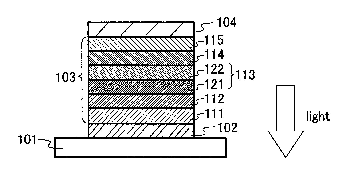
[0079]One mode of a light-emitting element of the present invention will be explained with reference to FIG. 1A.

[0080]The light-emitting element of the present invention includes a plurality of layers between a pair of electrodes. The plurality of layers is stacked in combination of a layer formed of a substance with a high carrier injecting property and a layer formed of a substance with a high carrier transporting property so that a light-emitting region is formed in a portion away from the electrodes, in other words, so that carriers are recombined in a portion away from the electrodes.

[0081]In this embodiment mode, a light-emitting element includes a first electrode 102, a second electrode 104, and an EL layer 103 provided between the first electrode 102 and the second electrode 104. Note that in this embodiment mode, explanation is made on the assumption that the first electrode 102 functions as an anode and the second electrode 104 functions as a cathode. That is, the explanat...

embodiment mode 2

[0141]In this embodiment mode, a mode of a light-emitting element of the present invention having a structure in which a plurality of light-emitting units is stacked (hereinafter, referred to as a stacked element) will be explained with reference to FIG. 4. This light-emitting element has a plurality of light-emitting units between a first electrode and a second electrode.

[0142]In FIG. 4, a first light-emitting unit 511 and a second light-emitting unit 512 are stacked between a first electrode 501 and a second electrode 502. The first electrode 501 and the second electrode 502 can be similar to those described in Embodiment Mode 1. In addition, the first light-emitting unit 511 and the second light-emitting unit 512 may have the same structure or different structures. Structures of the first light-emitting unit 511 and the second light-emitting unit 512 may be similar to the structure of the EL layer described in Embodiment Mode 1.

[0143]A charge generation layer 513 contains a compo...

embodiment mode 3

[0149]In this embodiment mode, a light-emitting device having a light-emitting element of the present invention will be explained.

[0150]In this embodiment mode, a light-emitting device having the light-emitting element of the present invention in a pixel portion will be explained with reference to FIGS. 5A and 5B. FIG. 5A is a top view of a light-emitting device, and FIG. 5B is a cross-sectional diagram taken along lines A-A′ and B-B′ of FIG. 5A. This light-emitting device includes a driver circuit portion (source side driver circuit) 601, a pixel portion 602, and a driver circuit portion (gate side driver circuit) 603 which are shown by dashed lines in order to control light emission of the light-emitting element. Reference numeral 604 denotes a sealing substrate, 605 denotes a sealant, and a portion surrounded by the sealant 605 is a space 607.

[0151]A lead wiring 608 is a wiring for transmitting signals to be inputted to the source side driver circuit 601 and the gate side driver ...


PUM


Abstract

A light-emitting element is provided which has a light-emitting layer between a first electrode and a second electrode, where the light-emitting layer has a first layer and a second layer; the first layer contains a first organic compound and a third organic compound; the second layer contains a second organic compound and the third organic compound; the first layer is provided to be in contact with the second layer on the first electrode side; the first organic compound is an organic compound with an electron transporting property; the second organic compound is an organic compound with a hole transporting property; the third organic compound has an electron trapping property; and light emission from the third organic compound can be obtained when voltage is applied to the first electrode and the second electrode so that the potential of the first electrode is higher than that of the second electrode.

Description

BACKGROUND OF THE INVENTION[0001]1. Field of the Invention[0002]The present invention relates to a current excitation light-emitting element, a light-emitting device, an electronic appliance each having the light-emitting element, and method of manufacturing the same.[0003]2. Description of the Related Art[0004]In recent years, a light-emitting element utilizing electroluminescence has been actively researched and developed. In a basic structure of such a light-emitting element, a substance with a light-emitting property is sandwiched between a pair of electrodes. When voltage is applied to this element, light emission can be obtained from the substance with a light-emitting property.[0005]Since such a light-emitting element is a self-luminous type, there are advantages in that it has higher visibility of pixels than liquid crystal displays, there is no need to use a backlight, and the like. Thus, such a light-emitting element is considered to be suitable as a flat panel display ele...

Claims


Application Information

Patent Timeline
Patent Type & Authority Applications(United States)
IPC IPC(8): H01L27/28B05D5/12
CPCH01L51/006H01L51/0067H01L51/008H01L51/0081H01L51/5203H01L51/0087H01L51/009H01L51/5012H01L51/0085H10K85/633H10K85/322H10K85/324H10K85/346H10K85/361H10K85/654H10K85/342H10K50/11C09K11/06H10K50/805
Inventor SAKATA, JUNICHIROINOUE, HIDEKOSEO, SATOSHIOHSAWA, NOBUHARU
Owner SEMICON ENERGY LAB CO LTD
Why Eureka
Try Eureka