
Method for Preparing Nano Metallic Particles

a nano-metal and nano-particle technology, applied in the direction of magnetic bodies, superimposed coating processes, transportation and packaging, etc., can solve the problems of complex fabrication process, and the array of nano-metal particles, so as to achieve high fabrication and time costs and lower costs

Inactive Publication Date: 2008-05-08
IND TECH RES INST
View PDF1 Cites 14 Cited by
  • Summary
  • Abstract
  • Description
  • Claims
  • Application Information

AI Technical Summary

Benefits of technology

The present invention provides a method for preparing nano metallic particles using an electroplating process. This method has the advantage of being a direct method with lower costs and larger process windows to control the distribution and size of the nano particles. The surface roughness of the conductive substrate after the surface treating process is of nano scale. The potential range applied during the electroplating process is designed to be close to the standard reduction reaction potential of the metallic ions, thereby controlling the nucleation sites. The cyclic number of the electroplating process is adjusted to control the growing size of the nano metallic particles, and therefore nano metallic particles with controllable size can be randomly formed on the conductive substrate. In addition, lithographic technology can be used to prefabricate conductive and non-conductive regions on the conductive substrate, and diversified nano metallic particle array layouts can be fabricated in the present invention.

Problems solved by technology

The conventional nano metallic particle array technologies all have disadvantages concerning complicated fabrication processes and high fabrication and time costs.

Method used


Image

  • Method for Preparing Nano Metallic Particles
  • Method for Preparing Nano Metallic Particles
  • Method for Preparing Nano Metallic Particles

Examples


Embodiment Construction

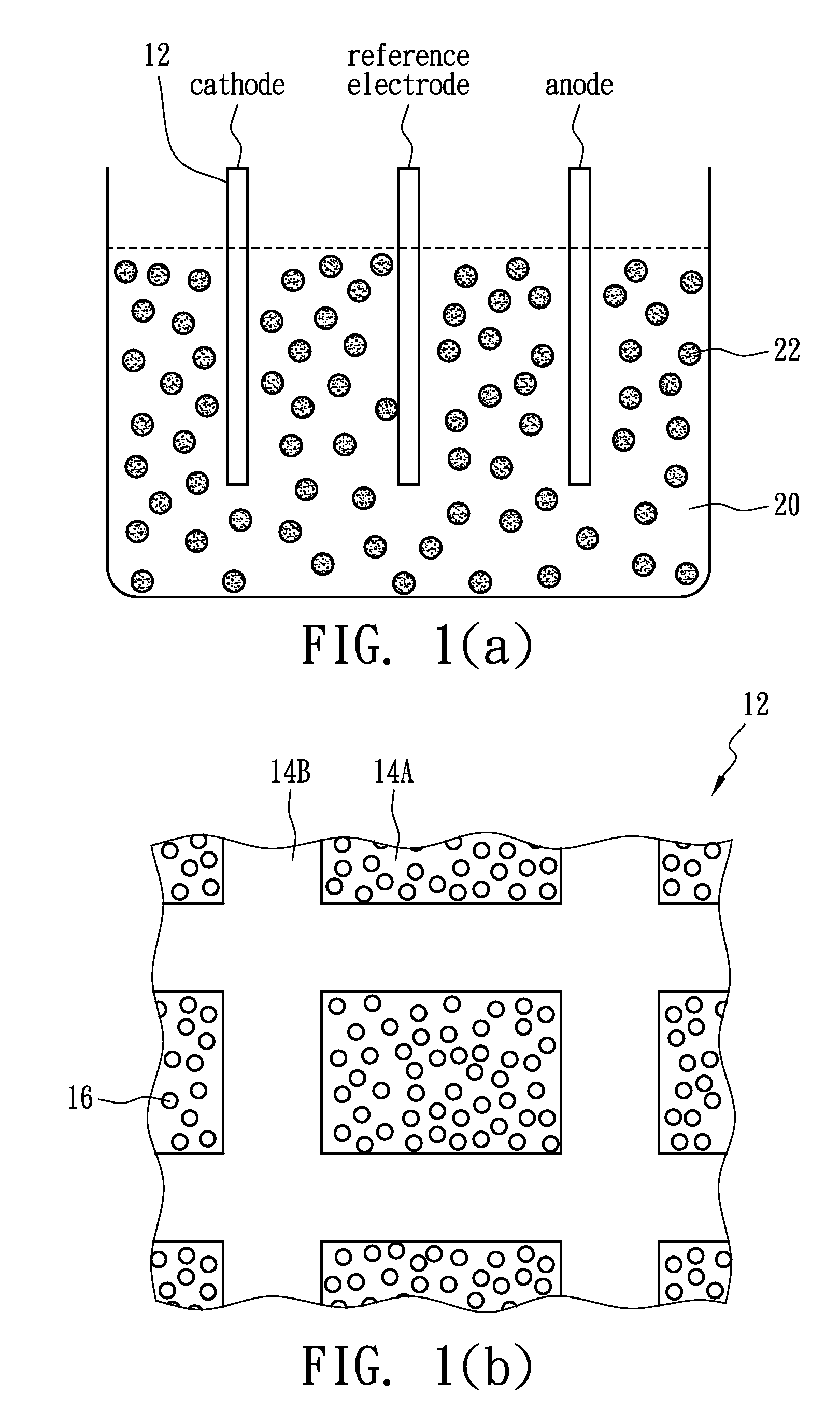
[0024]FIGS. 1(a) and 1(b) illustrate methods for preparing nano metallic particles 16 according to the present invention. A conductive substrate 12 is dipped in an electroplating solution 20 containing metallic ions 22, and an electroplating process (e.g., cyclic voltammery electroplating process) is then performed to form nano metallic particles 16 on the conductive substrate 12 by the reduction reaction of the metallic ions 22. Preferably, the size of the nano metallic particles 16 is between 1 nm and 150 nm. Preferably, the conductive substrate 12 includes indium-tin-oxide (ITO) with the lattice size between 5 nm and 500 nm. The electroplating solution 20 may include nickel nitrate, nickel sulfate or nickel chloride, and the nano s metallic particles 16 may be nickel metallic particle. In addition, the electroplating solution 20 may contain magnetic metallic ions such as iron ions or cobalt ion, and the nano metallic particles 16 may be magnetic metallic particles such as iron pa...


PUM

PropertyMeasurementUnit
surface roughnessaaaaaaaaaa
sizeaaaaaaaaaa

Abstract

A method for preparing nano metallic particles comprises the steps of dipping a conductive substrate in an electroplating solution containing metallic ions and performing an electroplating process to form the nano metallic particles on the conductive substrate by the reduction reaction of the metallic ions. The nano metallic particles can be used as a catalyst to perform a chemical vapor deposition process to form carbon nanotubes on the conductive substrate. Subsequently, fluorescent material can be positioned on the carbon nanotubes to form a light-emitting device. When a predetermined voltage is applied between the conductive substrate and the fluorescent material, the carbon nanotubes on the conductive substrate emit electrons due to the point discharge effect, and the electrons bombard the fluorescent material to emit light beams.

Description

BACKGROUND OF THE INVENTION[0001](A) Field of the Invention[0002]The present invention relates to a method for preparing nano metallic particles, and more particularly, to a method for preparing nano metallic particles by reducing metallic ions with an electroplating process.[0003](B) Descriptions of the Related Art[0004]Recently researchers have developed many nano metallic particle array technologies based on different principles, for example, electron beam writing method, anode alumina template method, micro-contact printing method and block macromolecular template method.[0005]Although the electron beam writing method (see Adv. Mater. 2003, 15, 49, Vol. 16, p. 3246, 2001) may randomly and precisely implant nano metallic particles, the writing process is quite time consuming and is not suitable for mass production processes requiring efficiency and large area. In additions, it is necessary for the electron beam writing method to use a complicated lithography etching process, and ...

Claims


Application Information

Patent Timeline
Patent Type & Authority Applications(United States)
IPC IPC(8): C23C28/02C25D5/48C25D3/12C25D3/20C25D5/00
CPCB22F2998/00B82Y25/00B82Y30/00C25D5/02C25D5/18C25D7/001C25D5/54H01F1/0045C25D5/34C25D7/006B22F1/0018C25D5/617B22F1/054B22F1/056
Inventor TSENG, YU TSANLIN, CHENG HSUANSHIAO, PO LING
Owner IND TECH RES INST
Learn More