
Method and apparatus for producing semiconductor films, photoelectric conversion devices and method for producing the devices

a technology of photoelectric conversion device and semiconductor film, which is applied in the direction of final product manufacture, sustainable manufacturing/processing, sulfur compounds, etc., can solve the problems of low selenium utilization efficiency, inability to achieve high conversion efficiency, and inability to achieve high selenium utilization efficiency compared to other source metals

Inactive Publication Date: 2008-03-27
NAT INST OF ADVANCED IND SCI & TECH
View PDF13 Cites 52 Cited by
  • Summary
  • Abstract
  • Description
  • Claims
  • Application Information

AI Technical Summary

Benefits of technology

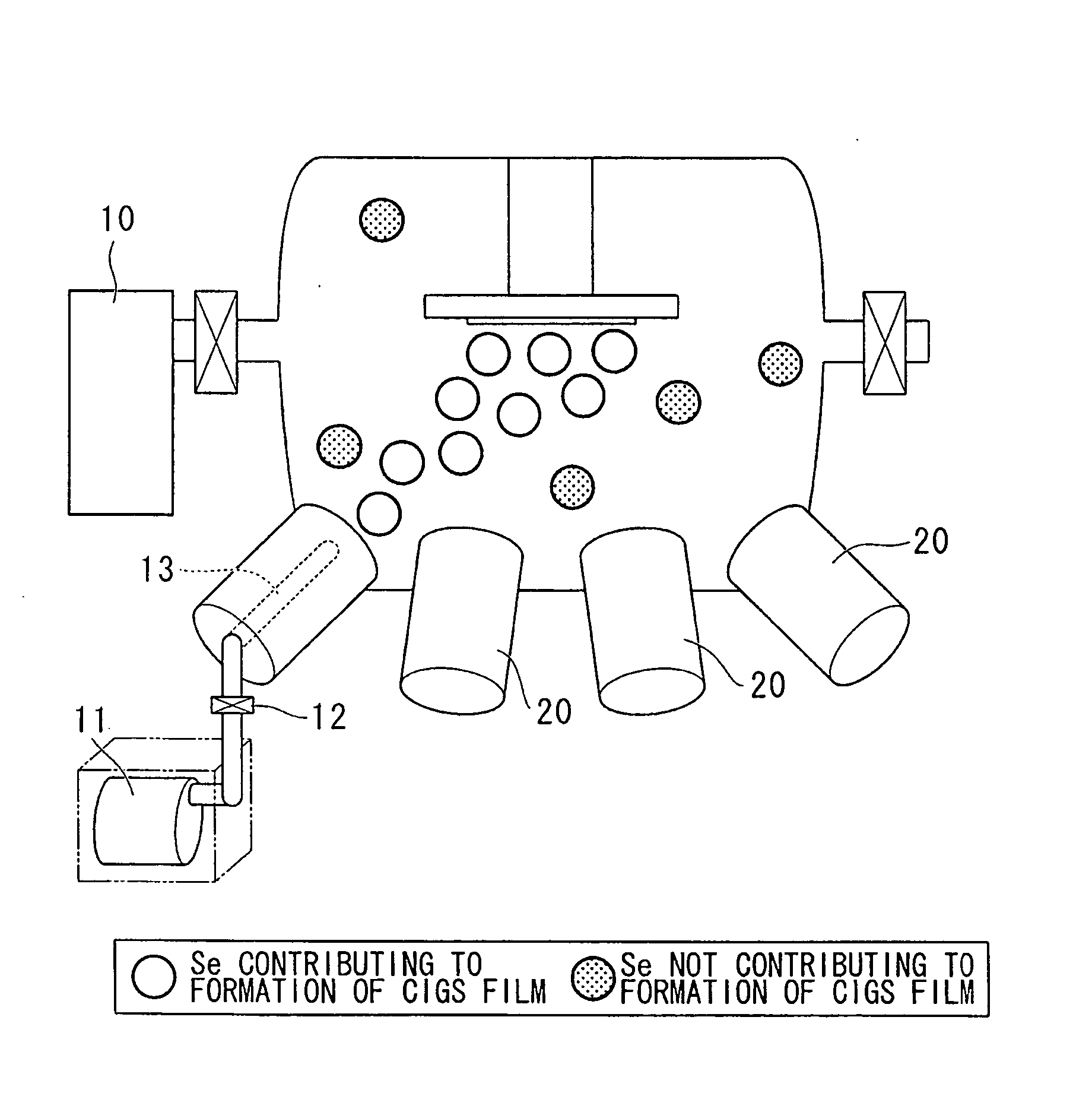
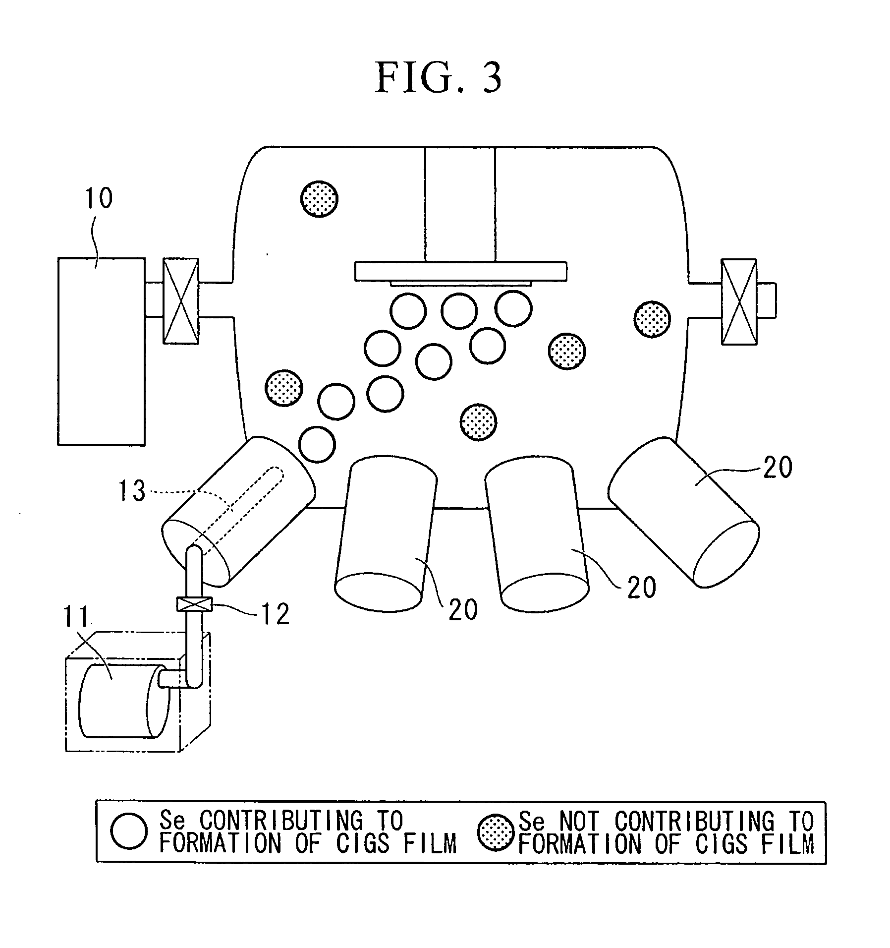
[0010] The present invention takes the above circumstances into consideration, with an object of providing a method for producing a semiconductor film having a chalcopyrite structure comprising a group Ib element, a group IIIb element and a group VIb element including Se and a method for producing a photoelectric conversion device, in which loss of the source selenium during the film production process of a semiconductor thin film such as a CIGS thin film and adhesion of selenium on the inner wall of the deposition chamber can be prevented or suppressed.

Problems solved by technology

Although the selenization method is known as a technique for manufacturing CIGS solar cells with a large area, it has problems in that a high conversion efficiency cannot be obtained.
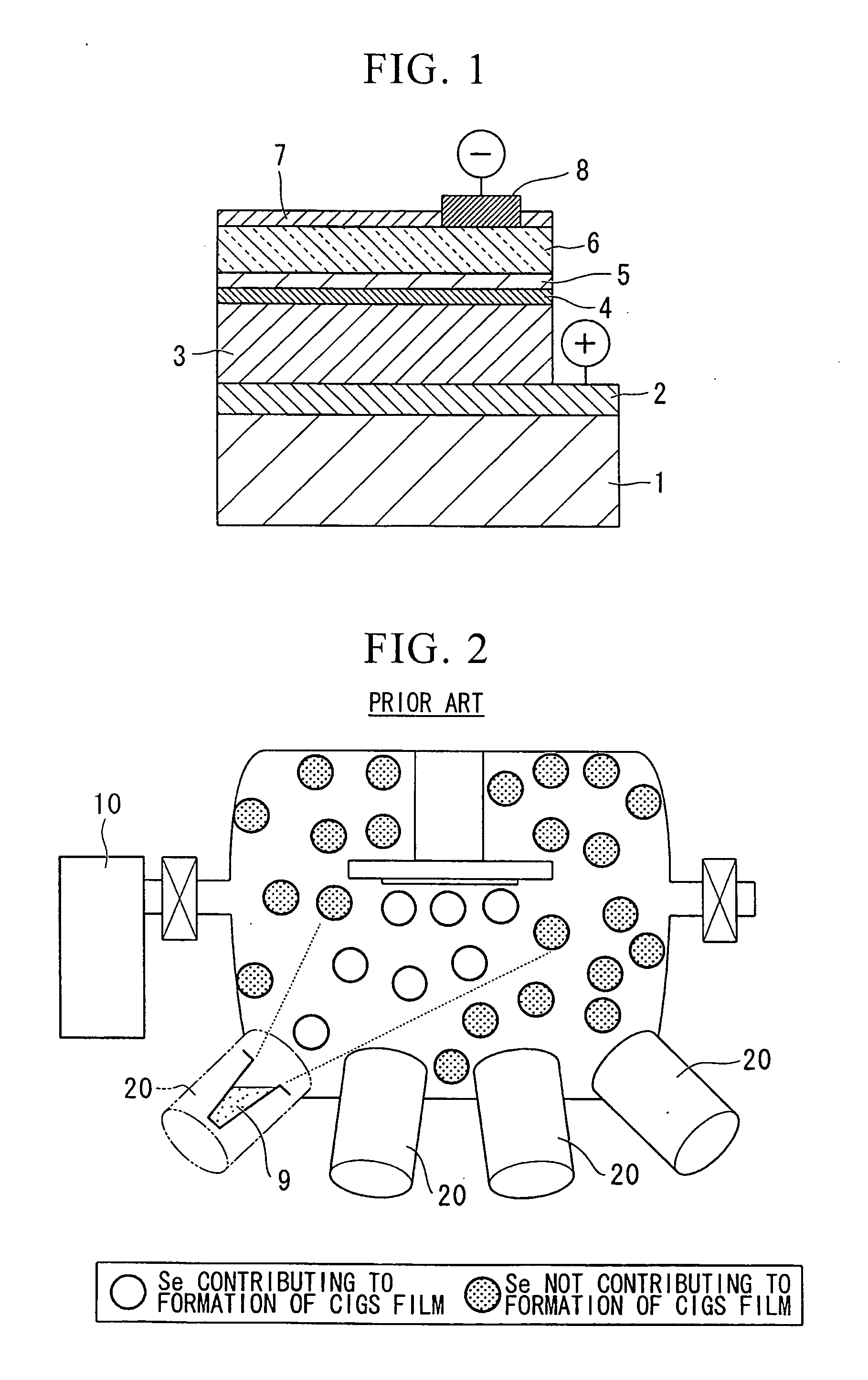
Therefore, the amount of selenium contributing to the actual production of a film is extremely small as compared to the amount of selenium supplied to the vapor source crucible, and most of the supplied selenium is adhered to the inner wall or the like of the deposition chamber, and not utilized.
As a result, a problem arises in that the utilization efficiency of the source selenium is markedly low as compared to other source metals.
Hence, the multi-source evaporation method was unsuitable for mass production.

Method used


Image

  • Method and apparatus for producing semiconductor films, photoelectric conversion devices and method for producing the devices
  • Method and apparatus for producing semiconductor films, photoelectric conversion devices and method for producing the devices
  • Method and apparatus for producing semiconductor films, photoelectric conversion devices and method for producing the devices

Examples


example 1

[0064] Using a vacuum deposition apparatus based on a molecular beam epitaxy apparatus having an effective film-production area of (10×10) cm and having a structure as shown in FIG. 3, CIGS thin films were produced under conditions wherein the distance between the Se source and the substrate was 30 cm, the film thickness was 1.8 μm, and the film-production rate was 0.7 μm / hr. The average consumption of source Se per one film production process was measured, and was found to be 5.08 g.

[0065] The electron micrograph of the surface of the CIGS thin film produced is shown in FIG. 5A.

example 2

[0070] Using a thin film according to the present invention, a CIGS solar cell having substantially the same structure as shown in FIG. 1 except for the antireflection film 7 was produced as follows.

[0071] A Mo back electrode was formed on a glass substrate having a size of 3 cm×3 cm by a sputtering method. Then, a CIGS thin film was formed in the same manner as in Example 1, and a CdS buffer layer was formed by a chemical bath deposition (CBD) method. Thereafter, a highly resistive zinc oxide layer and a transparent electrode layer were formed by a sputtering method. Finally, an Al grid electrode was formed by evaporation. In this manner, eight independent solar cells were produced on a glass substrate. The area of one independent solar cell was about 0.5 cm2.

[0072]FIG. 6 is a graph showing the current-voltage characteristic curve of a CIGS solar cell produced by the method of the present invention, wherein AM was 1.5. Despite the fact that the produced solar cell had no antirefl...


PUM

PropertyMeasurementUnit
Structureaaaaaaaaaa
Semiconductor propertiesaaaaaaaaaa

Abstract

A method for producing a semiconductor film having a chalcopyrite structure including a Ib group element, a IIIb group element and a VIb group element including selenium, the method including cracking selenium with plasma to generate radical selenium, and using the radical selenium in the process of forming the semiconductor film.

Description

[0001] The present invention claims priority on Japanese Patent Application No. 2006-228342, filed Aug. 24, 2006, and Japanese Patent Application No. 2007-150108, filed Jun. 6, 2007, the contents of which are incorporated herein by reference. BACKGROUND OF THE INVENTION [0002] 1. Field of the Invention [0003] The present invention relates to a method and apparatus for producing a semiconductor film, photoelectric conversion devices and method for producing the devices. More particularly, the present invention is related to a method and apparatus for producing a semiconductor film having a chalcopyrite structure, photoelectric conversion devices and method for producing the devices. [0004] 2. Description of Related Art [0005] A thin-film solar cell provided with a photovoltaic absorber layer including a semiconductor film having a chalcopyrite structure including a group Ib element, a group IIIb element and a group VIb element, which is represented by the formula: CuInSe2, or such a ...

Claims


Application Information

Patent Timeline
IPC IPC(8): H01L31/0272B01J19/00C01B19/00
CPCH01L31/072H01L31/0749C23C14/243C23C14/0026C23C14/0623Y02E10/541Y02P70/50
Inventor ISHIZUKA, SHOGONIKI, SHIGERUSAKURAI, KEIICHIROYAMADA, AKIMASAMATSUBARA, KOJI
Owner NAT INST OF ADVANCED IND SCI & TECH
Learn More