Epitaxial nucleation and buffer sequence for via-compatible InAs/AlGaSb HEMTs
a technology of inas/algasb hemts and buffer sequences, which is applied in the direction of basic electric elements, electrical apparatus, and semiconductor devices. it can solve the problems of low electron mobility, reduced threading dislocation, and high electron mobility
- Summary
- Abstract
- Description
- Claims
- Application Information
AI Technical Summary
Benefits of technology
Problems solved by technology
Method used
Image
Examples
Embodiment Construction
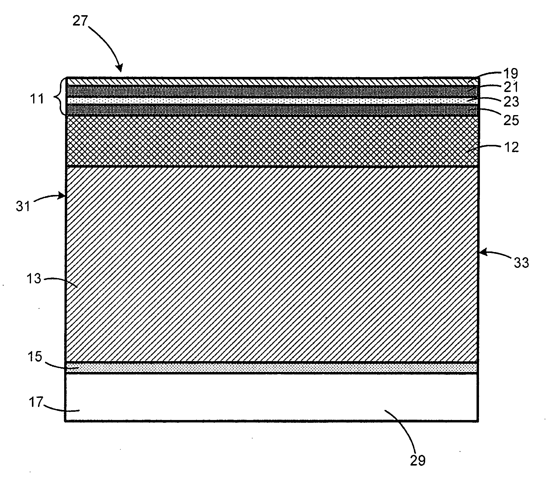
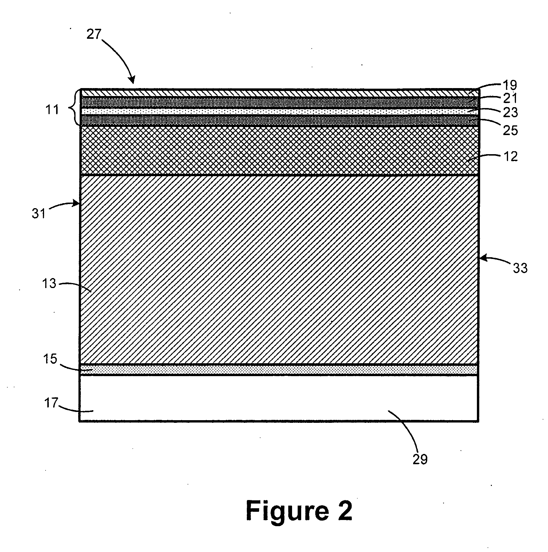
[0018]FIG. 2 is a cross-sectional view of a metamorphic HEMT (“mHEMT”), according to one embodiment of the invention. The mHEMT has a plurality of HEMT layers 11, a stabilizing layer 12, a metamorphic buffer layer 13, a nucleation layer 15, and a substrate wafer 17. The HEMT layers 11 include a metal layer 19, a first layer of barrier material 21, a layer of channel material 23, and a second layer of barrier material 25.
[0019]The metal layer 19 can be selectively deposited or removed to form a source (not shown), a drain (not shown) and a gate (not shown). The metal layer can have a thickness of about 0.1 to about 1 μm.
[0020]The barrier material 21 and 25 can be an Antimonide-based semiconductor, such as Aluminum Antimonide (AlSb), Gallium Antimonide (GaSb), or their respective alloys. AlSb barrier 21 and 25 has about 1.3 eV conduction band offset allowing for sheet carrier concentrations up to 1×1013 cm−2. Both AlSb and AlGaSb are stable compounds with insulating properties, and th...
PUM
 Abstract
Description
Claims
Application Information
 - R&D
- Intellectual Property
- Life Sciences
- Materials
- Tech Scout
- Unparalleled Data Quality
- Higher Quality Content
- 60% Fewer Hallucinations
Browse by: Latest US Patents, China's latest patents, Technical Efficacy Thesaurus, Application Domain, Technology Topic, Popular Technical Reports.
© 2025 PatSnap. All rights reserved.Legal|Privacy policy|Modern Slavery Act Transparency Statement|Sitemap|About US| Contact US: help@patsnap.com


