
In-situ process state monitoring of chamber

a technology of process state monitoring and chamber, which is applied in the direction of plasma technique, chemical vapor deposition coating, coating, etc., can solve the problems of wasting 200 testing silicon wafers for each 3,000 wafer processed, damage to the device, and surface residual contamination or residue level

Inactive Publication Date: 2008-03-13
APPLIED MATERIALS INC
View PDF9 Cites 183 Cited by
  • Summary
  • Abstract
  • Description
  • Claims
  • Application Information

AI Technical Summary

Benefits of technology

[0010]Once the spectral and/or composition data is generated, a current model of chamber conditions can be determined using that data. The current model can be compared with an ideal model of chamber conditions, such as by using a statistical comparison technique like multivariate primary component analysis. For the comparison, each of the conditi

Problems solved by technology

A problem with existing processes for manufacturing devices such as semiconductor chips is that certain contaminants can be present in the plasma and get deposited onto the surfaces and into films of these devices during manufacture, which can damage the devices.
After removing contaminants from these surfaces, however, there will be some level of residual contamination or residue on the surfaces due in part to the cleaning process.
The gas concentrations of each gaseous species in the bulk plasma have been shown to be sensitive to chamber conditions due to surface-plasma interactions, such as radical recombination and surface reaction rate variation, such that the deposition process, for example, does not deposit a material in an ideal way.
In this example, about 200 testing silicon wafers are wasted for each 3,000 wafers processed, simply due to the need to remove residue after a cleaning procedure.
While the relative expense may be acceptable, as each cycling wafer may be on the order of about $200 compared to around $10K for a patterned wafer involving 100-120 process steps, the cost still is higher than desired as the manufacturer typically runs more cycling wafers through the system than is needed.
This system downtime further increases the cost per chip and reduces throughput.

Method used


Image

  • In-situ process state monitoring of chamber
  • In-situ process state monitoring of chamber
  • In-situ process state monitoring of chamber

Examples


Embodiment Construction

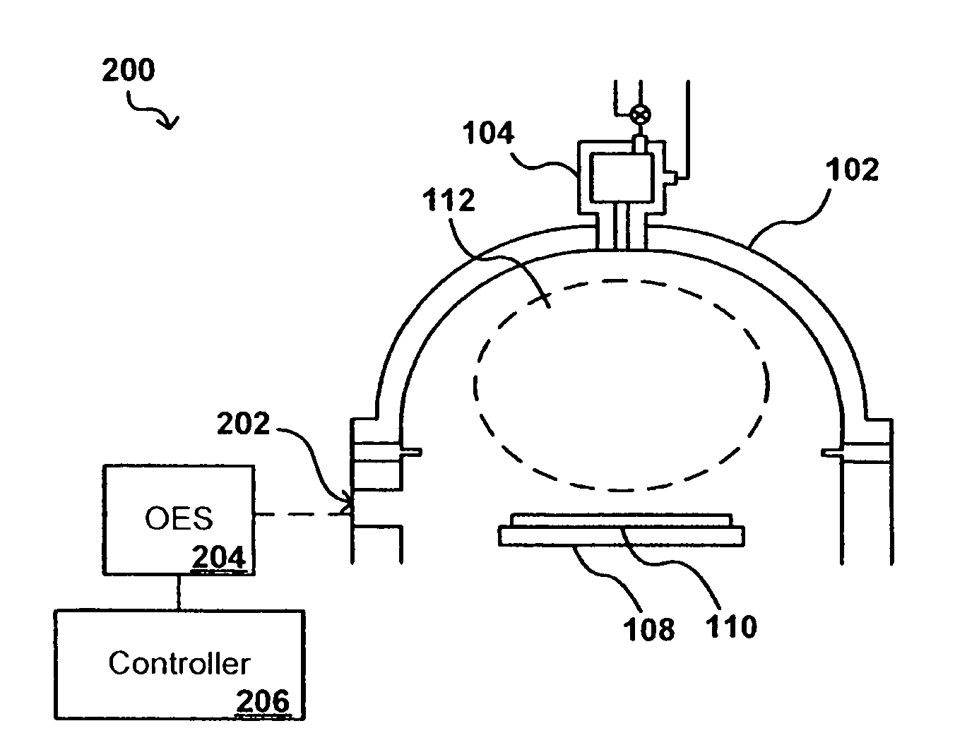
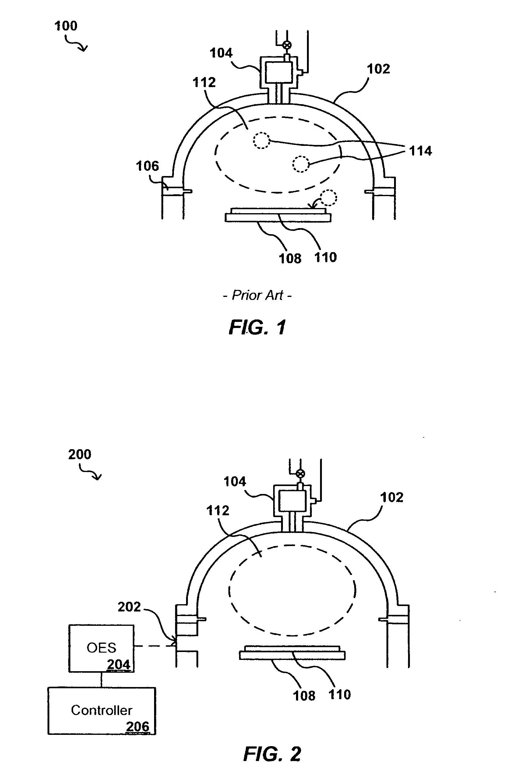
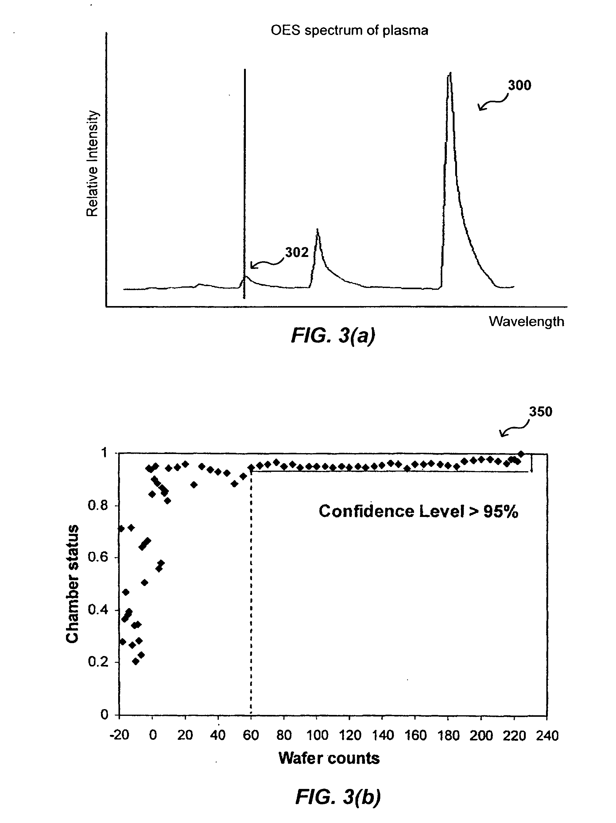
[0020]Systems and methods in accordance with various embodiments of the present invention can overcome the aforementioned and other deficiencies in existing processing systems by providing for in-situ process state monitoring for chamber conditions, such as a determination of plasma composition during processing, as well as after a process such as a preventative maintenance (PM) or other such process. In order to properly monitor the chamber conditions, an ideal model is created that matches ideal chamber conditions for the process. Through a calibration procedure, for example, it can be determined which values of each material component of a bulk plasma in the process chamber produce the best resulting material and / or device. These material components can include, for example, the reactive gases used for a deposition. This model then can be quantified for comparison as will be discussed later herein. For subsequent processing, a current model can be generated for the current chambe...


PUM

PropertyMeasurementUnit
Pressureaaaaaaaaaa
Compositionaaaaaaaaaa
Levelaaaaaaaaaa

Abstract

The process state of a chamber after a maintenance procedure can be monitored in-situ in order to ensure that the chamber is ready for processing, while minimizing waste and downtime due to aftereffects of the maintenance procedure. The composition of a bulk plasma in a process chamber can be analyzed using an analytical tool to capture the emission spectrum of the plasma. The spectrum can be analyzed to generate a model of the current chamber conditions, which can be compared to a model of ideal chamber conditions using a statistical analysis approach such as multivariate primary component analysis. If the current and ideal models match to within a set confidence level, the chamber conditions are acceptable for processing devices, and any processing of cycling workpieces or other plasma-cleansing processes can be stopped.

Description

BACKGROUND OF THE INVENTION[0001]The present invention relates to the processing of a workpiece such as a substrate or silicon wafer. More particularly, the invention relates to a method and apparatus for monitoring the composition of a plasma when an integrated circuit is manufactured using a plasma processing technique.[0002]One of the steps in the fabrication of modern semiconductor devices is the formation of a thin film on a semiconductor substrate through a chemical reaction of selected gases. One such deposition process is referred to as chemical vapor deposition (“CVD”). Conventional thermal CVD processes supply reactive gases to the surface of a substrate, where heat-induced chemical reactions take place to produce a desired film. Plasma-enhanced CVD techniques, on the other hand, promote excitation and / or dissociation of the reactant gases through the application of radio-frequency (“RF”), microwave, or other energy to a reaction zone near the substrate surface, thereby cr...

Claims


Application Information

Patent Timeline
IPC IPC(8): H05H1/24C23C16/00
CPCC23C16/4401H01J37/32972H01J37/32935C23C16/52
Inventor PARK, SOONAMLIANG, QIWEIQIANG, ZHONGLUBOMIRSKY, DMITRYLEE, YOUNG S.
Owner APPLIED MATERIALS INC
Learn More