
Micro-channel chip and a process for producing the same

a microchannel chip and microchannel technology, applied in the direction of resistive material coating, metallic material coating process, electrical equipment, etc., can solve the problems of difficult shape of the fine tube, inability to produce film masks, and method that is even more sophisticated and expensive than is required to form the main channel, so as to achieve the effect of lower cost and higher yield

Inactive Publication Date: 2008-03-06
AIDA ENG LTD
View PDF4 Cites 69 Cited by
  • Summary
  • Abstract
  • Description
  • Claims
  • Application Information

AI Technical Summary

Benefits of technology

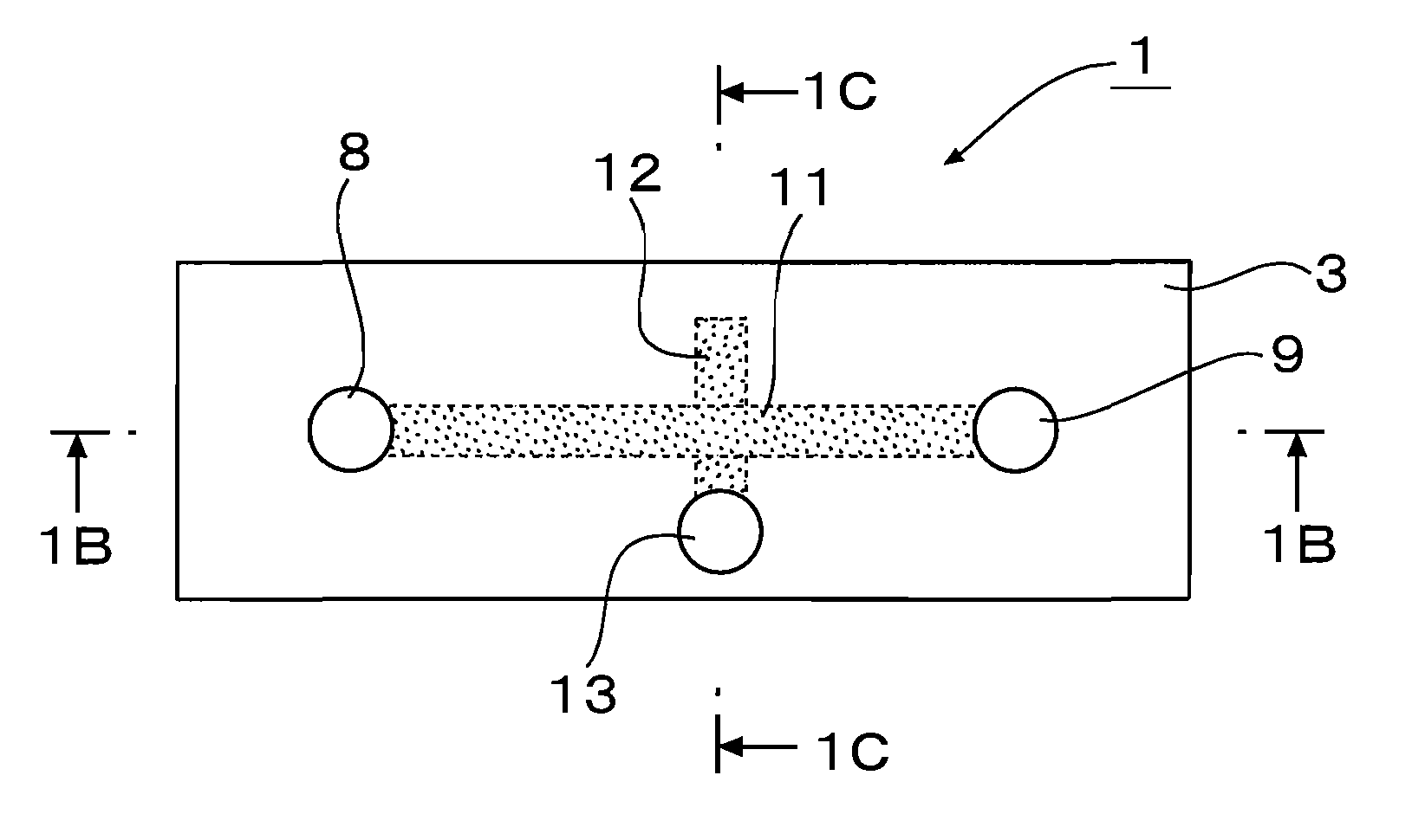
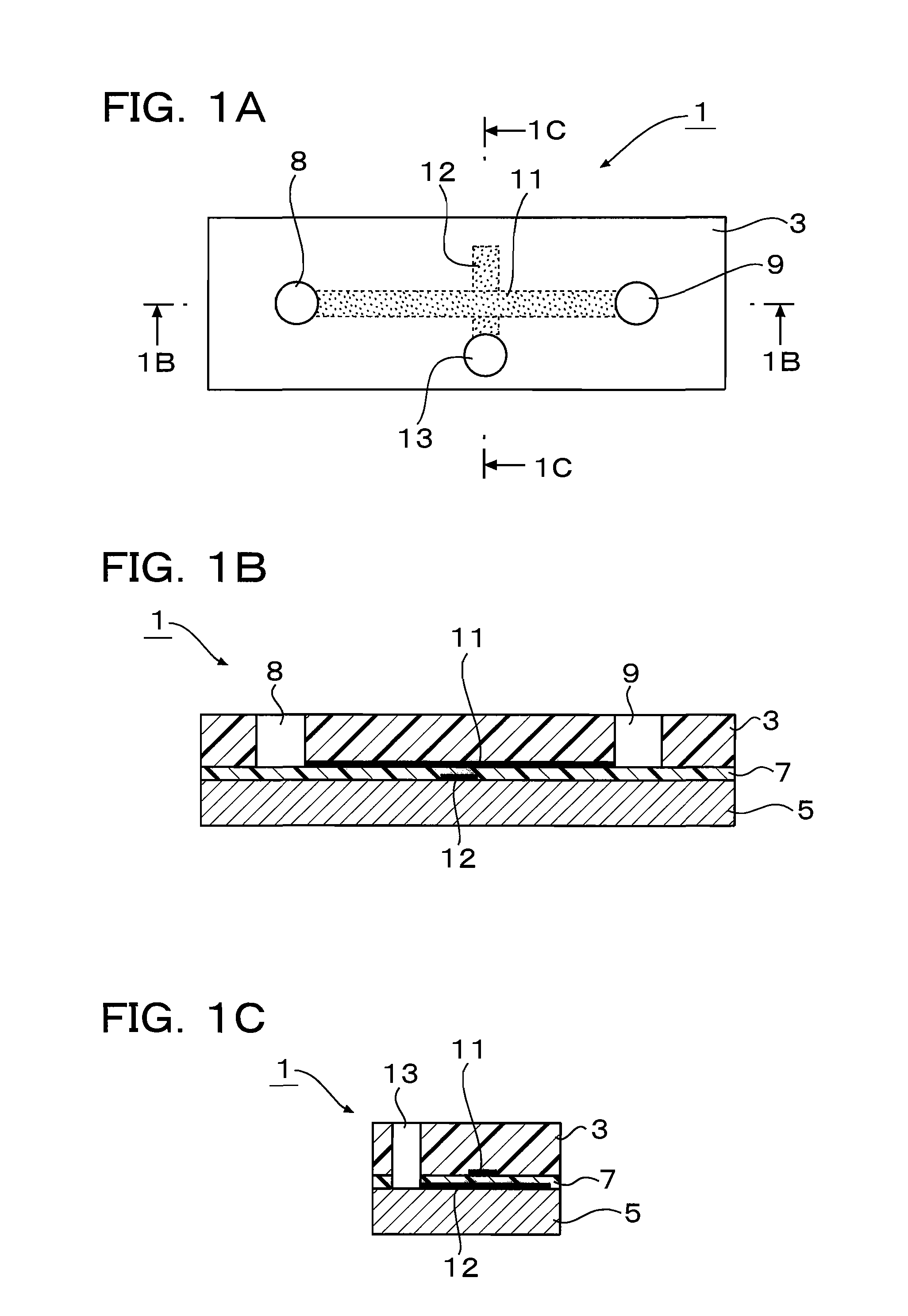
[0017] According to this embodiment, if a positive pressure is applied through one port on the non-adhesive thin-film layer for a micro-channel, that part of the substrate which corresponds to the non-adhesive thin-film layer for a micro-channel inflates to create a gap that can function as a micro-channel, whereupon it becomes possible to force a liquid and / or a gas from that port to the other port. If a positive pressure is applied through the pressure supply port on the non-adhesive thin-film layer for a shutter channel, that part of the intermediate substrate which corresponds to the non-adhesive thin-film layer for a micro-channel inflates to create a gap that can function as a shutter channel. Thus, by controlling the inflation of that part of the intermediate substrate which corresponds to the non-adhesive thin-film layer for a shutter channel, it can be operated to function as a micro-valve for opening or closing the upper micro-channel.
[0019] According to this embodiment, if a high positive pressure is applied through the pressure supply port on the non-adhesive thin-film layer for a shutter channel, that part of the intermediate substrate which corresponds to the non-adhesive thin-film layer for a shutter channel inflates to create a gap that can function as a shutter channel, whereupon the micro-channel having a fixed cross-sectional shape can be blocked. Thus, by controlling the inflation of that part of the intermediate substrate which corresponds to the non-adhesive thin-film layer for a shutter channel, it can be operated to function as a micro-valve for opening or closing the micro-channel having a fixed rectangular cross-sectional shape.
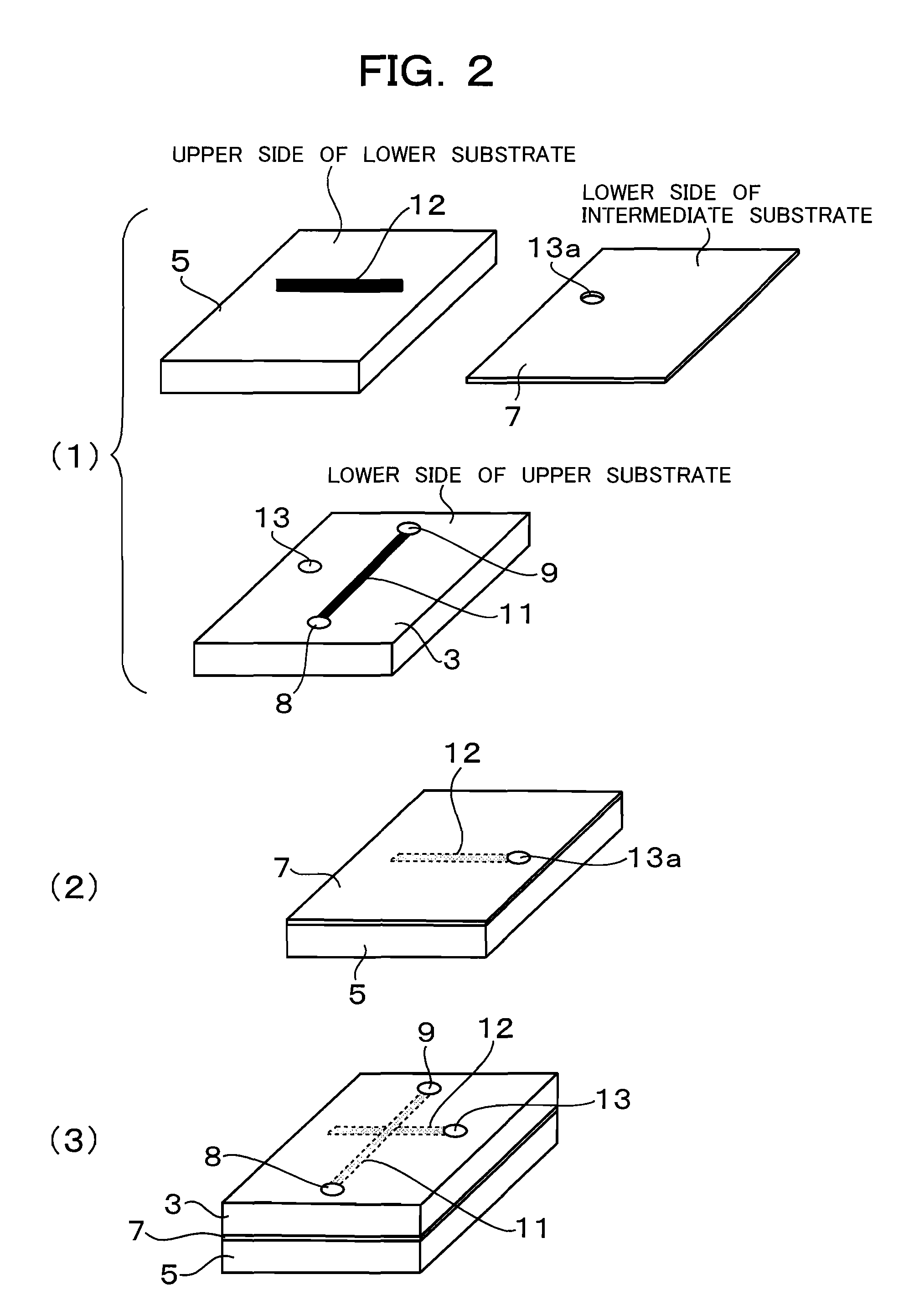
[0023] According to this embodiment, the linear, non-adhesive thin-film layer for a micro-channel and the non-adhesive thin-film layer for a shutter channel can be simultaneously formed on opposite sides of the same member, so the time required to achieve alignment when providing the two non-adhesive thin-film layers to intersect each other can be eliminated.
[0027] According to this embodiment, the non-adhesive thin-film layer that follows the mask pattern can be formed by simply depositing it on the mating side of a desired substrate and, hence, the micro-channel chip can be produced not only at lower cost but also in higher yield.
[0029] According to this embodiment, the non-adhesive thin-film layer is formed by printing, so the micro-channel chip can be produced not only at a much lower cost but also in a far higher yield.

Problems solved by technology

However, the micro-fluid control mechanism described in JP 2000-27813 A has the following problems.
(1) The Fine Tube is Difficult to Shape.
Hence, from the micro-forming viewpoint, the channel through the fine tube must be shaped by a method that is even more sophisticated and expensive than is required to form the main channel.
For instance, if lithography is used in micro-forming, a film mask is impracticable and an expensive glass mask must be employed.
(2) Channels cannot be Made Uniform in Height and it is Difficult to Fabricate the Intended Micro-Channel Chip.
In the case of forming fine channels as in a micro-channel chip, channels of equal height are easy to form but considerable difficulty is involved in fabricating channels of varying height.
But then the time required of substrate fabrication doubles and, what is more, the need to attach the two substrates together in high precision and other considerations that are introduced add to the difficulty involved in the fabrication of micro-channel chips.
(3) It is Difficult to Ensure that Only the Fine Tube Portion is Formed to have a Liquid-Repelling Nature.
With a fine structure, it is difficult to provide affinity for liquid in a part of the structure but make it repel liquid in another part.
If a liquid containing dust is suctioned through the fine tube, the dust might clog the inlet of the fine tube to make it no longer functional.
The dust may be so small that it will not cause clogging in the main channel but it might cause a problem in the fine tube.
These air bubbles might block the inlet of the fine tube, potentially depriving the fine tube of its ability to perform the intended function.
However, the micro-valve described in Japanese Patent No. 3418727 is of such a structure that the membrane (valve) which is detached from or attached to the valve seat simply makes a one-way displacement toward the pressure compartment and, hence, the membrane (valve), when it is in OPEN mode, will have only an insufficient gap from the valve seat, making the fluid less flowable and pulsate.
It is by no means easy to provide such a complex structure halfway down the micro-channel.

Method used


Image

  • Micro-channel chip and a process for producing the same
  • Micro-channel chip and a process for producing the same
  • Micro-channel chip and a process for producing the same

Examples


example 1

(1) Fabrication of Micro-Channel Chips

[0074] According to the flowchart shown in FIGS. 5A and 5B, a micro-channel chip 1B was fabricated. First, in step (a), two masks were prepared, each with a channel design punched through. Mask 20 was intended for the non-adhesive thin-film layer 11 and it was formed by cutting scores (feature size, 400 μm) through a PET film 0.025 mm thick to give a pattern of predetermined design. Mask 21 was intended for the non-adhesive thin-film layer 12 and it was formed by cutting scores (feature size, 400 μm) through a PET film 0.025 mm thick to give a pattern of predetermined design.

[0075] Next, in step (b), the mask 20 was placed on the lower side of the upper substrate 3 with a thickness of 3 mm that was made of silicone rubber (PDMS); the mask 20 was then attached to this upper substrate 3 by means of self-adsorption. The other mask 21 was placed on the upper side of the lower substrate 5 with a thickness of 3 mm that was made of silicone rubber (P...

example 2

(1) Fabrication of a Micro-Channel Chip

[0082] (a) Using a mold prepared by the usual procedure of photolithography, a silicone-rubber made upper substrate was formed; it was 3 mm thick and had a groove with a fixed rectangular shape as a micro-channel. The micro-channel (groove) was 400 μm wide and 50 μm deep. The lower side of the upper substrate and the upper side of a 100 μm thick silicone-rubber made intermediate substrate were subjected to a treatment for surface modification by the same method as in Example 1; the lower side of the upper substrate was attached to the upper side of the intermediate substrate, whereby the upper substrate was permanently bonded to the intermediate substrate. Three holes were bored through the permanently bonded assembly in predetermined positions.

[0083] (b) A mask was formed by cutting scores (feature size, 400 μm) through a PET film 0.025 mm thick to give a pattern of predetermined design. The mask was then placed on the upper side of a lower ...

example 3

(1) Fabrication of a Micro-Channel Chip

[0086] A micro-channel chip 1C of the design shown in FIG. 6 was fabricated. When a plurality of liquid chemicals are successively transferred through different channels into a single reaction chamber where they undergo intended reactions, the liquid chemical that has flowed through one channel into the reaction chamber might occasionally flow back into another channel. This phenomenon can be effectively prevented by using a micro-channel chip having the structure shown in FIG. 6. A PDMS upper substrate 3 having a thickness of 3 mm is provided with three ports 8-1, 8-2 and 8-3 that are through-holes for introducing a liquid. The upper substrate 3 is also provided with a through-hole 23 and a port 9; the through-hole 23 is for inflating an area that corresponds to a non-adhesive thin-film layer 25 in an enlarged region so as to create a reaction chamber, and the port 9 is a through-hole for discharging a liquid. Further, the upper substrate 3 i...


PUM

PropertyMeasurementUnit
Adhesivityaaaaaaaaaa

Abstract

A micro-channel chip comprising at least an upper substrate, a lower substrate, and an intermediate substrate interposed between the upper substrate and the lower substrate, at least one non-adhesive thin-film layer for a micro-channel being linearly formed on one mating side which is selected from among the mating sides of the upper substrate and the intermediate substrate and the mating sides of the lower substrate and the intermediate substrate, at least two ports being provided on the non-adhesive thin-film layer for a micro-channel, at least one non-adhesive thin-film layer for a shutter channel being linearly formed on the mating side opposite the mating side on which the non-adhesive thin-film layer for a micro-channel is formed such that it intersects the non-adhesive thin-film layer for a micro-channel by passing beneath or over the latter, with the intermediate substrate lying in between, and a pressure supply port for inflating that part of the substrate which corresponds to the non-adhesive thin-film layer for a shutter channel being provided in at least one area on the non-adhesive thin-film layer for a shutter channel.

Description

INCORPORATION BY REFERENCE [0001] The present application claims priority under 35 U.S.C. §119 to Japanese Patent Application No. 2006-141235 filed on May 22, 2006. The content of the application is incorporated herein by reference in its entirety. FIELD OF THE INVENTION [0002] The present invention relates to a micro-channel chip having a micro-fluid control element. More particularly, the present invention relates to a micro-channel chip having a micro-fluid control element that functions as a valve mechanism for controlling the flow of a fluid within a micro-channel. BACKGROUND [0003] Devices commonly known as “micro-total analysis systems (PTAS)” or “lab-on-chip” comprise a substrate and micro-structures such as micro-channels and ports that are provided in the substrate to form channels of specified shapes. It has recently been proposed that a variety of operations such as chemical reaction, synthesis, purification, extraction, generation and / or analysis be performed on substan...

Claims


Application Information

Patent Timeline
IPC IPC(8): B32B3/00B05D5/12C23F1/00
CPCB01L3/502738B01L2200/10B01L2200/12B01L2300/0816Y10T428/24612B01L2400/0487B01L2400/0638F16K99/0001B01L2300/087B01L2400/0655
Inventor HAGIWARA, HISASHIMISHINA, YOSHINORI
Owner AIDA ENG LTD
Learn More