Multi-station decoupled reactive ion etch chamber

Active Publication Date: 2008-01-17
ADVANCED MICRO FAB EQUIP INC CHINA
View PDF14 Cites 113 Cited by
  • Summary
  • Abstract
  • Description
  • Claims
  • Application Information

AI Technical Summary

Benefits of technology

[0014] A micro-channels ring structure is provided at the entrance to the evacuation path to help confine the plasma to the processing region, so that the plasma does not reach into the evacuation path and so that there is no crosstalk between the processing regions. The micro-channels also help in pressure distribution, since the single pump creates asymmetric pumping. The ring also prevents RF radiation leakage between the two processing regions. The ring is made so that the top portion is dielectric so there's no plasma sputtering, but the bottom is conductive and grounded to prevent RF leakage.
[0015] The plasma confinement of the subject chamber prevents beating, so that there is no need to have the RF power suppliers phase and frequency locked. Also, because of the plasma confinement and RF separation, either processing region may be operated alone, or both regions together.

Problems solved by technology

Consequently, such application need not have high accuracy of process uniformity over the wafer as more critical applications, such as semiconductor wafer etching.
Since the processing chamber is constructed so that there is no separation between the two wafers and no plasma can be ignited over the wafers, and further since a filter is provided to remove charged particles from the wafer processing chamber, the chamber of the '022 patent cannot be used for modern critical application, such as semiconductor wafer etching, but only for simple ashing.
While the solution of isolating the processing regions enables tandem processing of two wafers simultaneously, it introduces difficulties in what is commonly referred to as chamber matching or station matching.
That is, it becomes difficult to control the two processing regions of the chamber to provide identical plasma processing conditions.
For example, if one processing region develops higher etch rate than the other region, it becomes difficult to control the endpoint of the etch process.
On the other hand, if the end point is delayed, then the wafer at the higher etch rate region may be over etched and be damaged.
A modified version of this tandem chamber is disclosed in, e.g., U.S. Pat. No. 6,962,644, which teaches “a chamber defining a plurality of isolated processing regions.” In the '644 patent a “central pumping plenum” enables the two chambers “to communicate with each other,” which leads to a problem known in the art as RF “crosstalk.” RF cross talk is deleterious for tandem processing as conditions change in one processing region adversely effect the processing in the second tandem region.
The isolated tandem chambers described above still have the problem in that due to the isolation, it is hard to match the process results between the two processing regions.
This complicates the structure and construction of the chamber.
Finally, the method for generating plasma in the tandem chambers described above fail to provide the tight performance specifications required for fabricating advanced semiconductor devices.

Method used


Image

  • Multi-station decoupled reactive ion etch chamber
  • Multi-station decoupled reactive ion etch chamber
  • Multi-station decoupled reactive ion etch chamber

Examples


Embodiment Construction

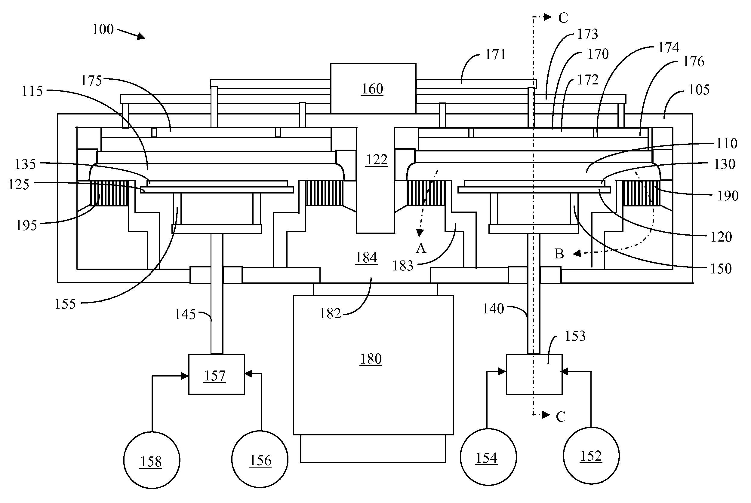
[0055] Embodiments of the subject invention provide a versatile plasma chamber enabling precision uniform processing at high throughput. The processing results conform to the high requirements of advanced semiconductor fabrication by combining various features and elements to enable stable and uniform plasma at each processing region. In particular, the combination of features as provided herein enable a multi-station decoupled reactive ion etch with multiple frequency RF power applied at each processing region. Various features and provisions are provided to avoid frequency beating and RF crosstalk between the two tandem processing regions. Notably, heretofore no tandem chamber has been proposed wherein decoupled RIE is enabled by the use of two RF frequencies fed from the cathode for each processing region.

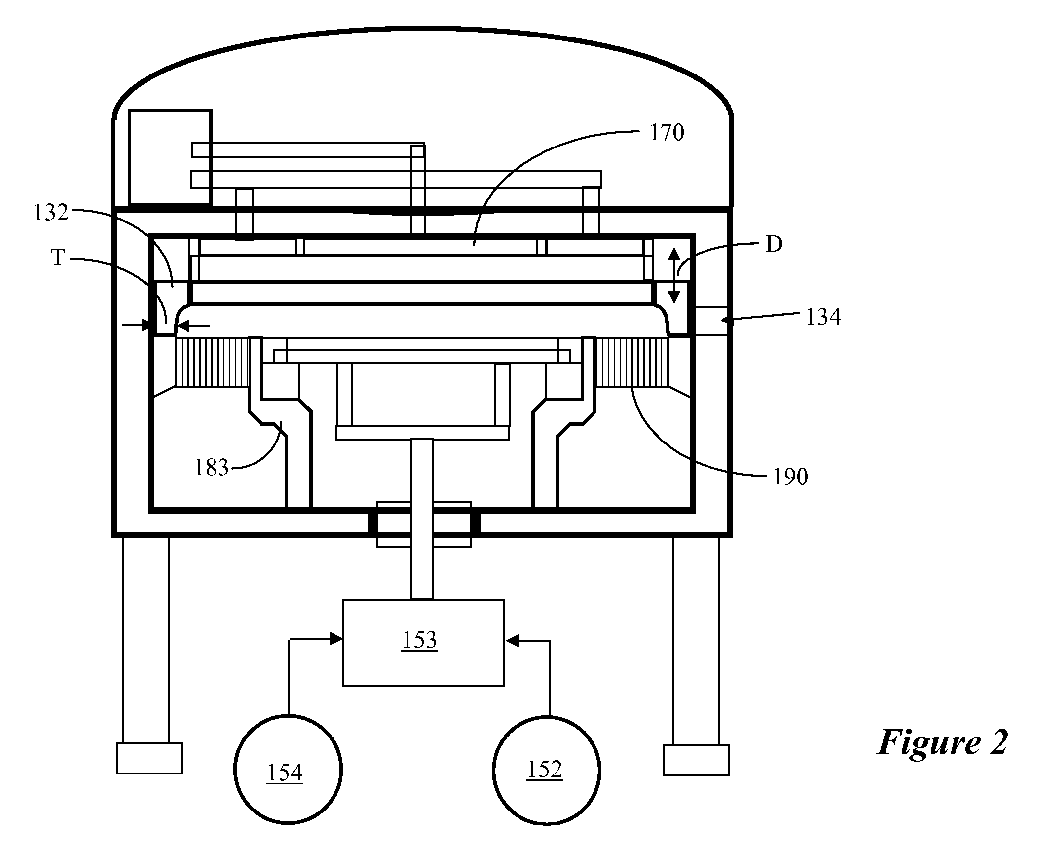
[0056]FIG. 1 is a schematic cross section of a tandem plasma chamber 100 according to an embodiment the invention, while FIG. 2 is a cross section along lines C-C of FIG. 1. Th...


PUM

PropertyMeasurementUnit
Frequencyaaaaaaaaaa
Frequencyaaaaaaaaaa
Frequencyaaaaaaaaaa

Abstract

A tandem processing-zones chamber having plasma isolation and frequency isolation is provided. At least two RF frequencies are fed from the cathode for each processing zones, where one frequency is about ten times higher than the other, so as to provide decoupled reactive ion etch capability. The chamber body is ground all around and in-between the two processing zones. The use of frequency isolation enables feed of multiple RF frequencies from the cathode, without having crosstalk and beat. A plasma confinement ring is also used to prevent plasma crosstalk. A grounded common evacuation path is connected to a single vacuum pump.

Description

RELATED APPLICATIONS [0001] This application is a continuation-in-part of U.S. application, Ser. No. 11 / 441,290, filed May 24, 2006, which in turn claims priority from Chinese Patent Application, Serial Number 200510028567.0, filed on Aug. 5, 2005, the disclosures of both of which are incorporated herein by reference in their entirety. This application also claims priority from Chinese Patent Application, Serial Number 200710042285.5, filed on Jun. 20, 2007.BACKGROUND [0002] 1. Field of the Invention [0003] The subject invention relates to plasma processing chambers and, more specifically, to plasma processing chambers having at least twin or tandem processing regions enabling processing of at least two substrates simultaneously. [0004] 2. Related Art [0005] In the fabrication of semiconductor wafers, two types of semiconductor processing systems are commonly employed. The first type of systems commonly used is generally referred to as batch processing systems. The chief reason behi...

Claims


Application Information

Patent Timeline
IPC IPC(8): C23F1/00H05H1/00
CPCH01J37/32091H01J37/32165H01J2237/334H01J37/32642H01J37/32183H01J37/32623H01J37/32633H01J37/32889H01J37/32899H01L21/67161H01L21/67173H01L21/6719
Inventor YIN, GERALDNI, TUQIANGCHEN, JINYUANQIAN, XUEYU
Owner ADVANCED MICRO FAB EQUIP INC CHINA
Why Eureka
Try Eureka