Coating layer thickness measurement mechanism and coating layer forming apparatus using the same
a coating layer and measurement mechanism technology, applied in the direction of apparatus for force/torque/work measurement, electrical/magnetic thickness measurement, instruments, etc., can solve the problem of difficult rotation of the electrode, the thickness of the coating cannot be changed or occurrence of damage, and the thickness of the coating cannot be free of variation or damage, etc. problem, to achieve the effect of suppressing the variation in the speed of feeding a base material, minimizing the influence of the sway of the measurement surfa
- Summary
- Abstract
- Description
- Claims
- Application Information
AI Technical Summary
Benefits of technology
Problems solved by technology
Method used
Image
Examples
first example
[0027][Formation of Si Vapor-Deposited Layer on Metal Foil Tape]
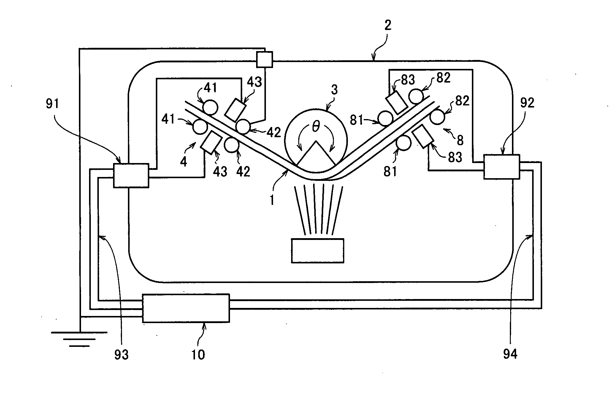
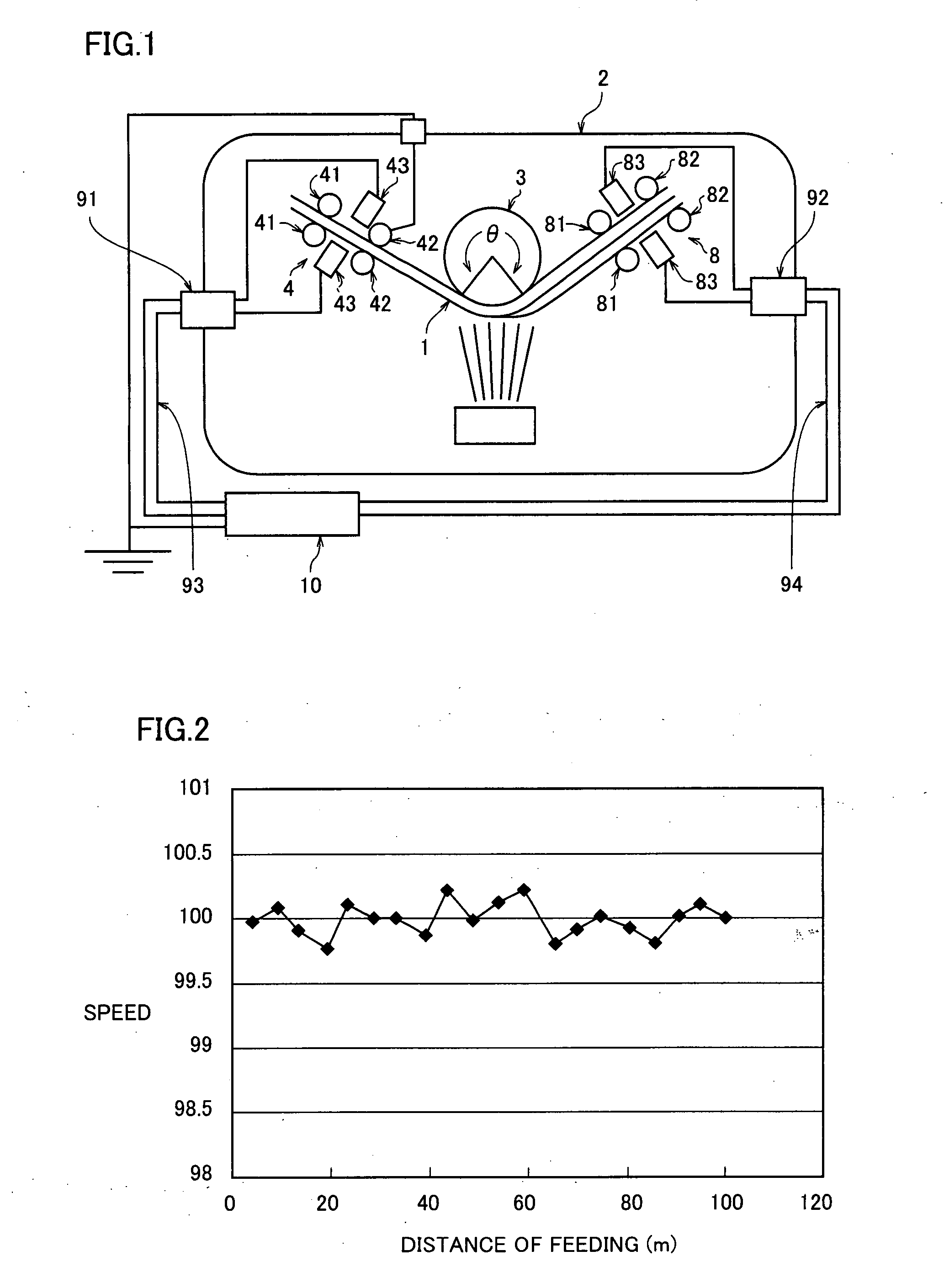
[0028]Referring to FIG. 1, a base material 1 formed as a conductive film is fed from a supply side roller (not shown) placed outside a vacuum chamber 2 on the right in the drawing to a roller 3 in the treatment base station placed inside the vacuum chamber, and an Si vapor-deposited layer or the like is formed on the surface thereof. Thereafter, base material 1 is wound and recovered by a recovery side roller (not shown) placed outside the vacuum chamber on the left in the drawing. The supply side roller is driven, for example, by a motor through an electromagnetic torque control mechanism, and set to transmit tension T1 of force in the direction opposite to the feeding direction to base material 1. On the other hand, the recovery side roller is driven by a motor through an electromagnetic torque control mechanism, and set to transmit tension T2 of force in the feeding direction to base material 1. Roller 3 at the treat...
second example
[0036][Formation of Various Vapor-Deposited Layers on Metal Foil Tape and Feedback of Measurement Value to Manufacturing System]
[0037]Base Material 1, that is Formed as Pure Copper Foil, has a Width of 130 mm, a thickness of 10 μm, a length of 500 m, and surface roughness Ra of 2 μm, and was used in the first example, was prepared. The conditions substantially the same as in the first example were set, tension T3 to be applied at sensing portion 4, 8 was set to 200 MPa, and layers of various materials shown in the field of material for “coating layer” in Table 2 were vapor-deposited on the base material surface to an average thickness of approximately 5 μm.
[0038]If the specific resistance of the material is greater than a specific resistance of a semiconductor region, change in capacitance ΔC (ΔC / Δp) due to change in specific resistance Δρ becomes smaller, and change in thickness value Δt measured by the capacitance-type sensor also becomes smaller. Therefore, according to the measu...
PUM
| Property | Measurement | Unit |
|---|---|---|
| Ra | aaaaa | aaaaa |
| Ra | aaaaa | aaaaa |
| Ra | aaaaa | aaaaa |
Abstract
Description
Claims
Application Information
 - R&D
- Intellectual Property
- Life Sciences
- Materials
- Tech Scout
- Unparalleled Data Quality
- Higher Quality Content
- 60% Fewer Hallucinations
Browse by: Latest US Patents, China's latest patents, Technical Efficacy Thesaurus, Application Domain, Technology Topic, Popular Technical Reports.
© 2025 PatSnap. All rights reserved.Legal|Privacy policy|Modern Slavery Act Transparency Statement|Sitemap|About US| Contact US: help@patsnap.com


