
Method of manufacturing interconnect substrate

a technology of interconnection and substrate, which is applied in the direction of superimposed coating process, resistive material coating, liquid/solution decomposition chemical coating, etc., can solve the problem of difficulty in forming a minute interconnection pattern by electroless plating

Inactive Publication Date: 2007-09-20
SEIKO EPSON CORP
View PDF11 Cites 11 Cited by
  • Summary
  • Abstract
  • Description
  • Claims
  • Application Information

AI Technical Summary

Benefits of technology

[0030]According to one embodiment of the invention, there is provided a method of manufacturing an interconnect substrate having a linear interconnect by electroless plating without using a plating resist, the method comprising:

Problems solved by technology

However, since electroless plating reaction, in which a metal is deposited on a catalyst layer, does not occur when the area of the catalyst layer is not sufficiently large, it is difficult to form a minute interconnect pattern by electroless plating.

Method used


Image

  • Method of manufacturing interconnect substrate
  • Method of manufacturing interconnect substrate
  • Method of manufacturing interconnect substrate

Examples


first embodiment

1. First Embodiment

[0052]A first embodiment of the invention is described below.

1.1. METHOD OF MANUFACTURING INTERCONNECT SUBSTRATE

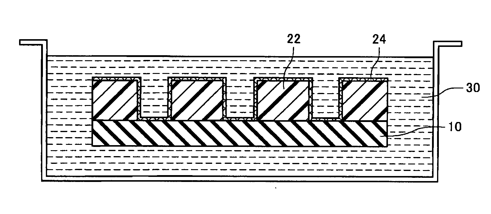
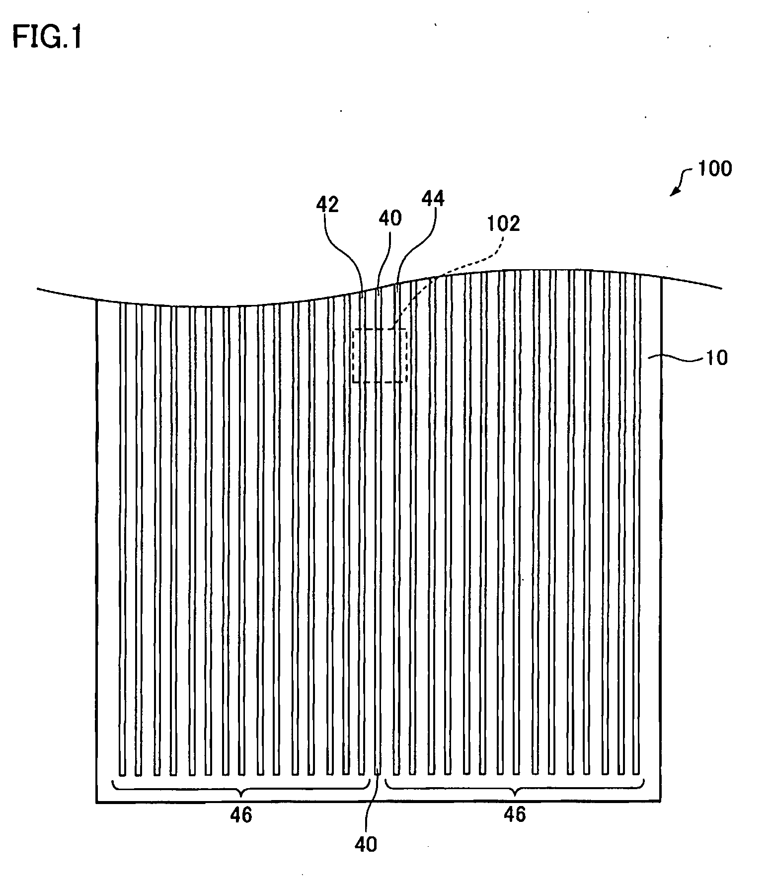
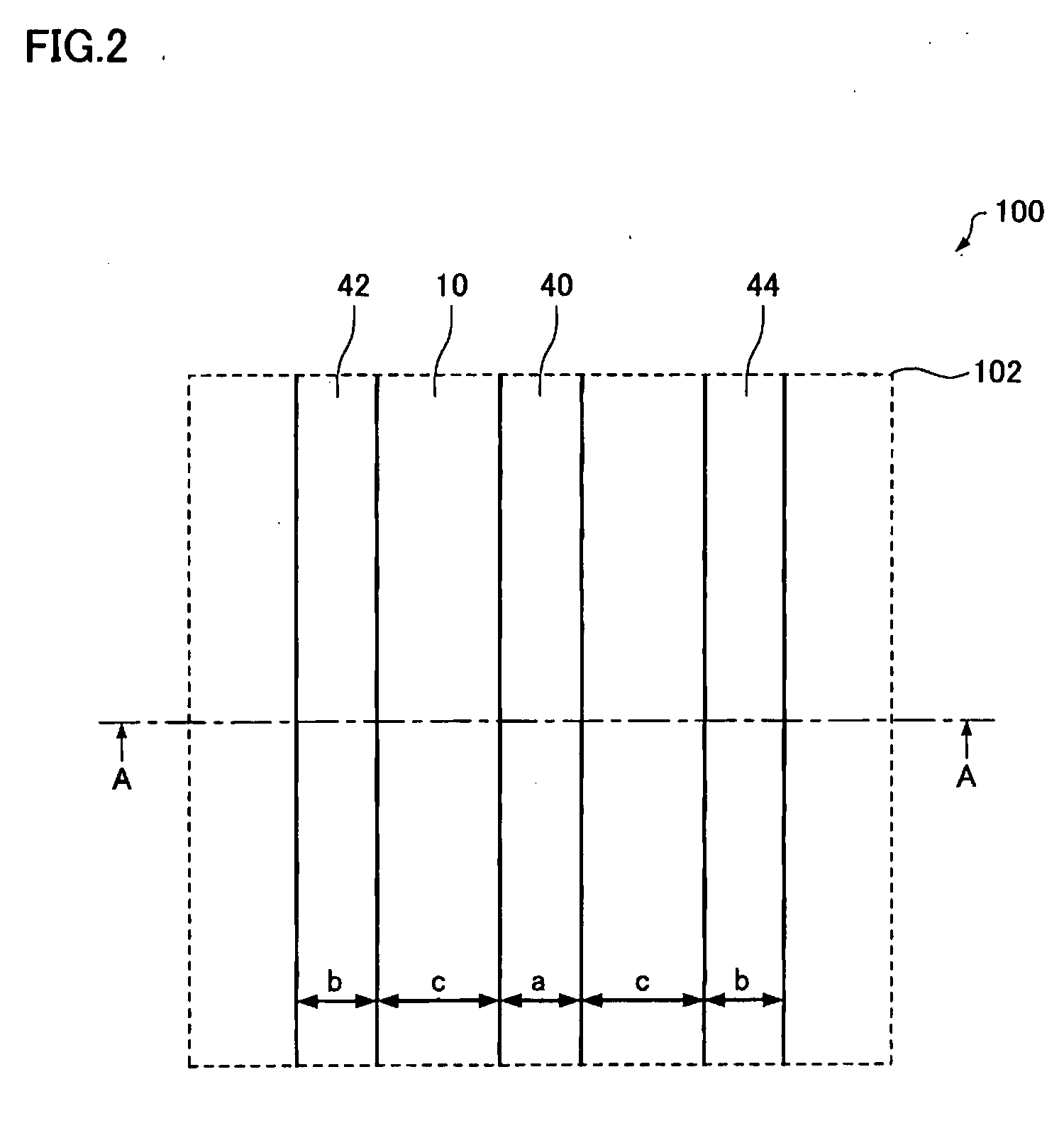
[0053]FIGS. 1 to 10 are diagrams showing an example of a method of manufacturing an interconnect substrate 100 (see FIG. 10) according to the first embodiment. FIGS. 1 and 2 are plan diagrams showing an example of the method of manufacturing an interconnect substrate according to the first embodiment. FIG. 2 is an enlarged diagram of a region 102 shown in FIG. 1. FIGS. 3 to 10 are cross-sectional diagrams of the interconnect substrate taken along the line A-A in FIG. 2.

[0054](1) A substrate 10 is provided. The substrate 10 may be an insulating substrate, as shown in FIG. 3. The substrate 10 may be an organic substrate (e.g. plastic material or resin substrate) or an inorganic substrate (e.g. quartz glass, silicon wafer, or oxide layer). As examples of the plastic material, polyimide, polyethylene terephthalate, polycarbonate, polyphenylene sulfide, and t...

second embodiment

4. Second Embodiment

4.1. INTERCONNECT SUBSTRATE

[0090]A second embodiment is described below. An interconnect substrate 200 according to the second embodiment differs from the interconnect substrate 100 according to the first embodiment as to the planar shape of the catalyst layer and the metal layer formed. FIG. 14 is a plan diagram showing a method of manufacturing an interconnect substrate according to the second embodiment. FIG. 14 corresponds to FIG. 1.

[0091]In the interconnect substrate 200, the catalyst layers 32 and the metal layers 34 are formed in pad-shaped (island-like) regions 240 and 242, as shown in FIG. 14. The regions 240 and 242 may be separated, as shown in FIG. 14. The catalyst layer formed in at least one of the regions 240 and 242 may have a square planar shape with a side length of 2 micrometers or less, and may have an area of 4 square micrometers or less. This region is preferably enclosed by a plurality of catalyst layers, and may be the region 240. The tota...


PUM

PropertyMeasurementUnit
widthaaaaaaaaaa
widthaaaaaaaaaa
widthaaaaaaaaaa

Abstract

A method of manufacturing an interconnect substrate having a linear interconnect by electroless plating without using a plating resist, the method including: (a) forming a plurality of rows of linear catalyst layers on a substrate; and (b) depositing a metal on the linear catalyst layers by electroless plating to form a plurality of rows of linear metal layers, at least one of the rows of linear catalyst layers having a line width of 2 micrometers or less, and a total line width of the linear catalyst layers on the substrate being 10 micrometers or more.

Description

[0001]Japanese Patent Application No. 2006-65991, filed on Mar. 10, 2006, is hereby incorporated by reference in its entirety.BACKGROUND OF THE INVENTION[0002]The present invention relates to a method of manufacturing an interconnect substrate.[0003]Electroless plating has attracted attention as a method of manufacturing an interconnect substrate. In electroless plating, a metal is deposited by reducing metal ions in an electroless plating solution by the function of a reducing agent. Therefore, since it is unnecessary to cause current to flow through the solution, a metal can also be deposited on an insulating substrate. Along with a recent increase in density of electronic instruments, it has become necessary to form a minute interconnect pattern by electroless plating.[0004]However, since electroless plating reaction, in which a metal is deposited on a catalyst layer, does not occur when the area of the catalyst layer is not sufficiently large, it is difficult to form a minute in...

Claims


Application Information

Patent Timeline
Patent Type & Authority Applications(United States)
IPC IPC(8): B05D5/12B28B19/00
CPCC23C18/30C23C18/32H05K3/048H05K3/184C23C18/2086H05K2203/0565C23C18/1608C23C18/1893H05K2201/09781
Inventor KIMURA, SATOSHIFURIHATA, HIDEMICHIKANEDA, TOSHIHIKO
Owner SEIKO EPSON CORP
Learn More