
Low profile semiconductor package-on-package

a technology of low-profile, semiconductor, applied in semiconductor devices, semiconductor/solid-state device details, electrical apparatus, etc., can solve the problems that the simple approach is no longer acceptable in recent applications, especially for hand-held wireless equipment, and achieves excellent electrical performance, shorten the time-to-market of innovative products, and mechanical stability. the effect of high product reliability

Inactive Publication Date: 2007-09-20
TEXAS INSTR INC
View PDF7 Cites 38 Cited by
  • Summary
  • Abstract
  • Description
  • Claims
  • Application Information

AI Technical Summary

Benefits of technology

[0005] Applicants recognize the need for a fresh push to shrink semiconductor devices both in two and in three dimensions, especially for a device-stacking and package-on-package method for semiconductor devices as well as electronic systems. Furthermore, it is hoped that a successful strategy for stacking chips and packages would shorten the time-to-market of innovative products, which utilize available chips of various capabilities (such as processors and memory chips) and would not have to wait for a redesign of chips. The device can be the base for a vertically integrated semiconductor system, which may include integrated circuit chips of functional diversity. The resulting system should have excellent electrical performance, mechanical stability, and high product reliability. Further, it will be a technical advantage that the fabrication method of the system is flexible enough to be applied for different semiconductor product families and a wide spectrum of design and process variations.

Problems solved by technology

This simple approach, however, is no longer acceptable for the recent applications especially for hand-held wireless equipments, since these applications place new, stringent constraints on the size and volume of semiconductor components used for these applications.

Method used


Image

  • Low profile semiconductor package-on-package
  • Low profile semiconductor package-on-package
  • Low profile semiconductor package-on-package

Examples


Embodiment Construction

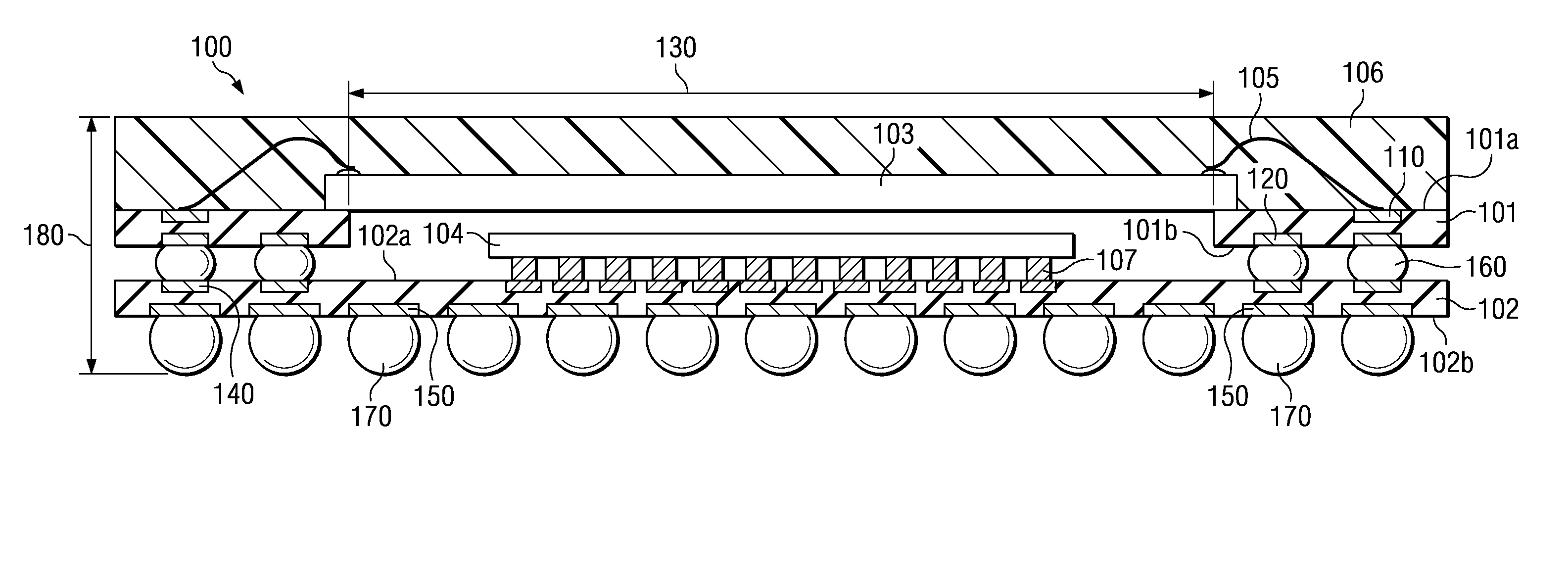
[0018]FIG. 1 is an example of an embodiment of the present invention, illustrating a vertically integrated semiconductor system with two substrates intended for connection to external parts. Due to an opening in one of the substrates for facilitating the system integration, the system has a low profile.

[0019] In FIG. 1, the system generally designated 100 has a first substrate 101 and a second substrate 102. First substrate 101 is made of an insulating body, has a first surface 101a and a second surface 101b, electrical contact pads 110 on the first surface, electrical contact pads 120 on the second surface, and a central opening of width 130. Preferred materials for substrate 101 are ceramics or polymers in a sheet-like configuration; the polymers may be stiff or compliant. The substrates have a thickness in the range from about 50 to 500 μm.

[0020] The second substrate 102 has a third surface 102a and a fourth surface 102b, electrical contact pads 140 on the third surface, and co...


PUM


Abstract

A semiconductor system (100) with two substrates has a first substrate (101) with a first and a second surface, electrical contact pads (110, 120) on the first and the second surface, and a central opening (130). The second substrate (102) has a third and a fourth surface, and electrical contact pads (140, 150) on the third and the fourth surface. Metal reflow bodies (160) connect the pads (120, 140) on the second and the third surface. A first semiconductor chip (103), or chip stack, is on the first surface over the opening (130), and a second semiconductor chip (104), or chip stack, is on the third surface inside the opening.

Description

FIELD OF THE INVENTION [0001] The present invention is related in general to the field of semiconductor devices and processes, and more specifically to low profile, vertically integrated package-on-package semiconductor systems. DESCRIPTION OF THE RELATED ART [0002] The thickness of today's semiconductor package-on-package products is the sum of the thicknesses of the semiconductor chips, electric interconnections, and encapsulations, which are used in the individual devices constituting the building-blocks of the products. This simple approach, however, is no longer acceptable for the recent applications especially for hand-held wireless equipments, since these applications place new, stringent constraints on the size and volume of semiconductor components used for these applications. [0003] Consequently, the market place is renewing a push to shrink semiconductor devices both in two and in three dimensions, and this miniaturization effort includes packaging strategies for semicond...

Claims


Application Information

Patent Timeline
IPC IPC(8): H01L23/02
CPCH01L23/13H01L2924/18165H01L25/105H01L2224/16145H01L2224/16225H01L2224/32145H01L2224/48225H01L2224/73207H01L2224/73265H01L2225/0651H01L2225/06513H01L2225/06568H01L2924/01079H01L2924/15311H01L2224/45144H01L25/0657H01L2924/15151H01L2225/1058H01L2225/1023H01L2225/1088H01L2224/32225H01L2224/48227H01L2924/00012H01L2924/00H01L24/73H01L2924/14
Inventor GERBER, MARK A.
Owner TEXAS INSTR INC
Learn More