
Layered crossbar for interconnection of multiple processors and shared memories

a crossbar and shared memory technology, applied in the field of interconnection architecture, can solve the problems of affecting the performance of graphics systems with a large number of processors, affecting the performance of graphics systems, and requiring many complex calculations to be executed when creating realistic or complex images, etc., and achieves low latency memory and processor scalability.

Inactive Publication Date: 2007-09-06
MIND FUSION LLC
View PDF25 Cites 116 Cited by
  • Summary
  • Abstract
  • Description
  • Claims
  • Application Information

AI Technical Summary

Benefits of technology

[0009] Advantages that can be seen in implementations of the invention include one or more of the following. Implementations enable low latency memory and processor scalability in graphics systems such as ray-tracing or rendering farms with currently available packaging and interconnect technology.

Problems solved by technology

However, many complex calculations must be executed when creating realistic or complex images.
Some images may take days to compute even when using a computer with a fast processor and large memory banks.
Because graphics calculations tend to be memory intensive applications, some multiple processor graphics systems are outfitted with multiple, shared memory banks.
However, conventional crossbar-based architectures do not scale well for a graphics system with a large number of processors.
Typically, the size of a crossbar switch is limited by processing and / or packaging technology constraints such as the maximum number of pins per chip.

Method used


Image

  • Layered crossbar for interconnection of multiple processors and shared memories
  • Layered crossbar for interconnection of multiple processors and shared memories
  • Layered crossbar for interconnection of multiple processors and shared memories

Examples


Embodiment Construction

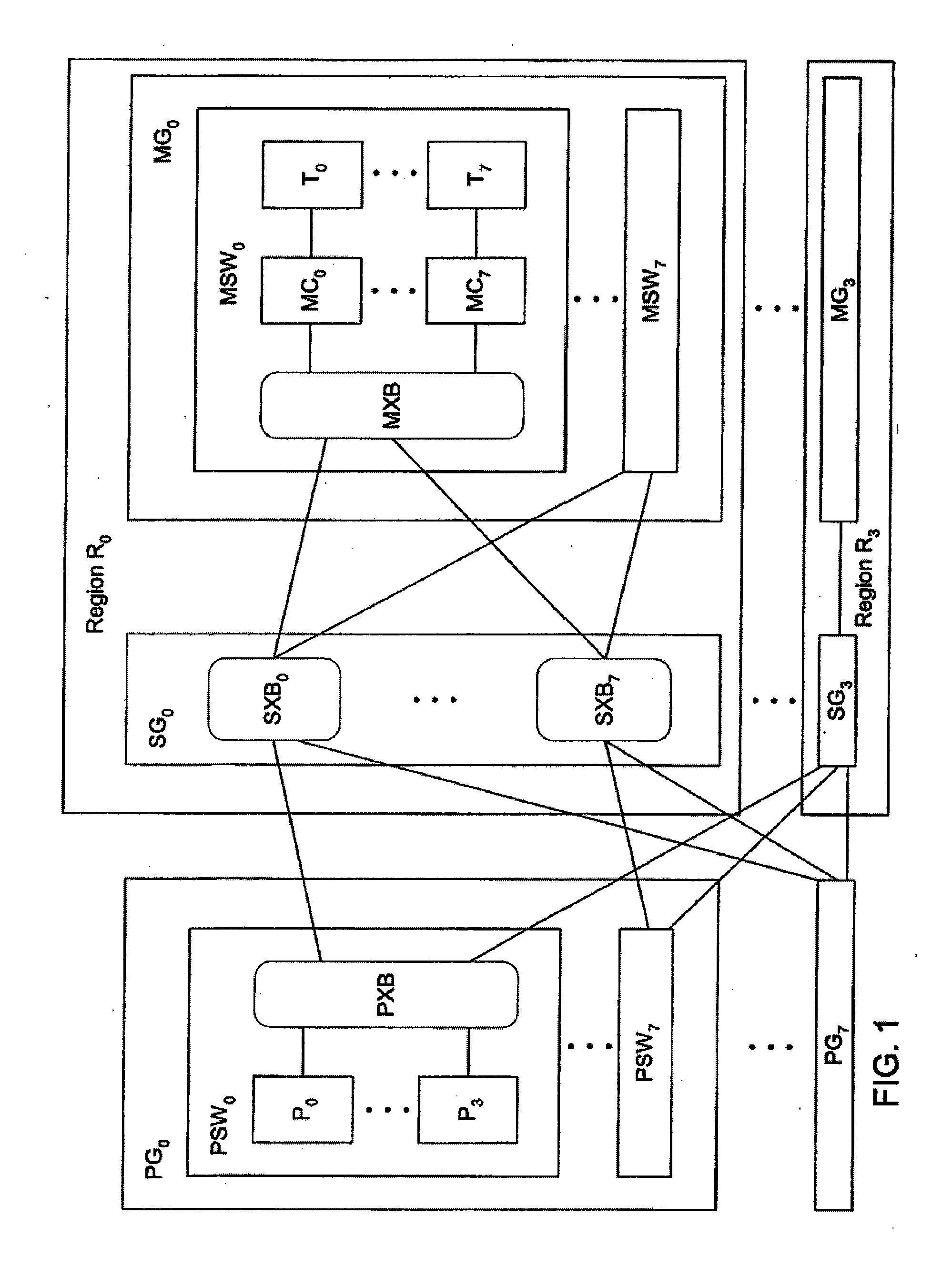
[0034]FIG. 1 illustrates an implementation with multiple memory switches. As shown in FIG. 1, a processor switch PSW is connected to a plurality of memory switches MSWA through MSWK by a plurality of external busses. Processor switch PSW includes a plurality of processors PA through PM. Each processor P is connected to a processor crossbar PXB by an internal bus.

[0035] Each memory switch MSW includes a plurality of memory controllers MCA through MCJ. Each memory controller MC is connected to a memory crossbar MXB by an internal bus. Each processor crossbar PXB is connected to a plurality of memory crossbars MXB.

[0036] Processor crossbar PXB provides full crossbar interconnection between processors P and memory crossbars MXB. Memory crossbars MB provide full crossbar interconnection between memory controllers MC and processor crossbar PXB.

[0037] In one implementation, each of processor switch PSW and memory switches MSW is fabricated as a separate semiconductor chip. One advantage...


PUM


Abstract

A method and apparatus includes a plurality of processor groups each having a plurality of processor switch chips each having a plurality of processors and a processor crossbar, each processor connected to the processor crossbar; a plurality of switch groups each having a plurality of switch crossbar chips each having a plurality of switch groups each having a plurality of switch crossbar chips each having a plurality of switch crossbars each connected to a processor crossbar in each processor group, wherein no two switch crossbars in a switch group are connected to the same processor crossbar; a plurality of memory groups having a plurality of memory switch chips each having a plurality of memory controllers and a memory crossbar, each memory controller connected to the memory crossbar, each memory crossbar in each memory group connected to all of the switch crossbar in a corresponding one of the switch groups, wherein no two memory groups are connected to the same switch group.

Description

CROSS-REFERENCES TO RELATED APPLICATIONS [0001] This application is a continuation of U.S. patent application Ser. No. 11 / 023,969, filed Dec. 27, 2004, which is a continuation of U.S. patent application Ser. No. 09 / 925,137, filed Aug. 8, 2001, which claims the benefit under 35 U.S.C. § 119(e) of U.S. Provisional Patent Application No. 60 / 304,933, filed Jul. 11, 2001, the disclosures of which are all incorporated herein by reference in their entirety for all purposes.BACKGROUND OF THE INVENTION [0002] The present invention relates generally to interconnection architecture, and particularly to interconnecting multiple processors with multiple shared memories. [0003] Advances in the area of computer graphics algorithms have led to the ability to create realistic and complex images, scenes and films using sophisticated techniques such as ray tracing and rendering. However, many complex calculations must be executed when creating realistic or complex images. Some images may take days to ...

Claims


Application Information

Patent Timeline
IPC IPC(8): G06F13/00G06F12/00G06F13/16G06F13/40G06F15/173
CPCG06F13/1657G06F15/17375G06F13/4022
Inventor PURCELL, STEPHEN CLARKCHENG, CHRISTOPHER THOMAS
Owner MIND FUSION LLC
Learn More