Inspecting circuit layout for LCD panel and fabricating method for LCD panel

Inactive Publication Date: 2007-09-06
CHUNGHWA PICTURE TUBES LTD
View PDF11 Cites 13 Cited by
  • Summary
  • Abstract
  • Description
  • Claims
  • Application Information

AI Technical Summary

Benefits of technology

[0012] An object of the invention is to provide an inspecting circuit layout, adapted for shortening the inspecting time for an individual panel unit or individual group of panel units.
[0013] Another object of the invention is to provide a method for fabricating LCD panel, for shortening the light inspection of LCD panels of a same batch.

Problems solved by technology

However, having maintained an on state for a long time, the active elements are likely to have characteristics variations and may not operate properly.
However, the inspecting method can inspect only one group of panel unit in one time.
Although using more probes may allow more groups of panel units to be inspected at same time and shorten the inspecting time, the corresponding inspecting cost is also increased.

Method used


Image

  • Inspecting circuit layout for LCD panel and fabricating method for LCD panel
  • Inspecting circuit layout for LCD panel and fabricating method for LCD panel
  • Inspecting circuit layout for LCD panel and fabricating method for LCD panel

Examples


first embodiment

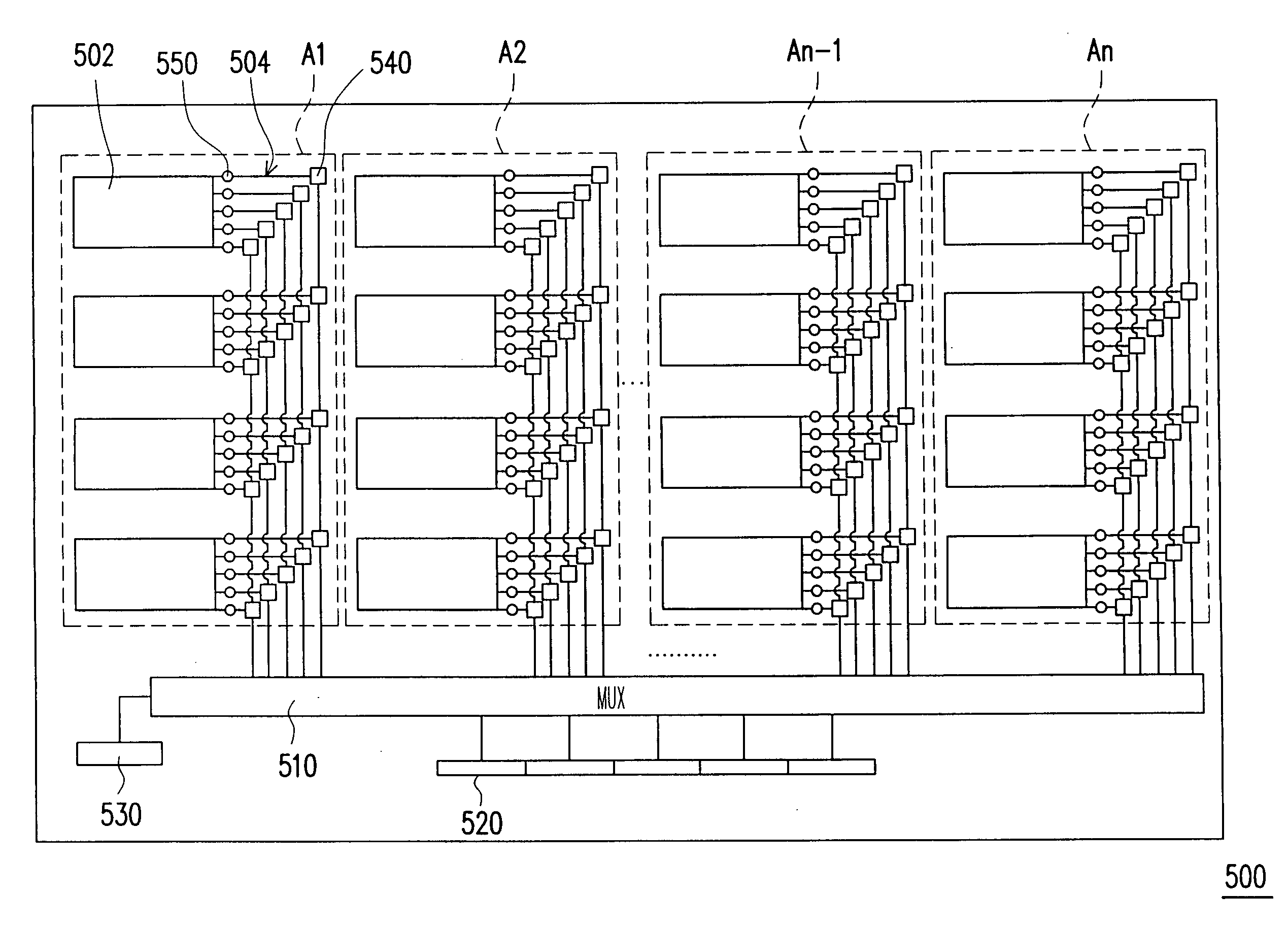
[0039]FIG. 4 is a schematic view of an inspecting circuit layout for panel unit according to the invention. Referring to FIG. 4, the inspecting circuit layout 500 is adapted for inspecting a plurality of panel units 502. Each of the panel units 502 includes a plurality of first signal lines 504a and second signal lines 504b, respectively. The panel units 502 receive input inspecting signals from the inspecting circuit layout 500 via the first signal lines 504a and the second signal lines 504b. In this embodiment, the first signal lines 504a are the scan lines, and the second signal lines 504b are the data lines.

[0040] As shown in FIG. 4, the inspecting circuit layout 500 includes a MUX 510 and an inspecting pad 520. The inspecting pad 520 is adapted for receiving inspecting signals for inspecting the panel units 502, and is electrically connected to the MUX 510. The MUX 510 is electrically connected between the inspecting pad 520 and the first signal lines 504a of the panel units 50...

third embodiment

[0051]FIG. 7 is a schematic view of an inspecting circuit layout for panel unit according to the invention. Referring to FIG. 7, except the MUX 510 and the inspecting pad 520 illustrated in the foregoing embodiment, the inspecting circuit layout 700 further includes a MUX 710 and a group of inspecting pads 720. In this embodiment, the panel units 502 are arranged in a matrix. Wherein, the MUX 510 is adapted for selectively conducting the inspecting pad 520 and the first signal line 504a (the scan line) of the panel unit 502 in some column; the MUX 710 is adapted for selectively conducting the inspecting pad 720 and the second signal line 504b (the data line) of the panel unit 502 in some row. As shown in FIG. 8, the components of the MUX 710 are almost the same as that of the MUX 510, and the MUX 710 also comprises control transistors 712 and refresh signal supplying units 760 electrically connected to the refresh transistors 714.

[0052] Please refer to FIGS. 5, 7 and 8, in this embo...


PUM


Abstract

An inspecting circuit layout according to the present invention is provided. The inspecting circuit layout is adapted for inspecting panel units group by group, each of the panel units having a plurality of first and second signal lines. The inspecting circuit layout includes a multiplexer (MUX) and an inspecting pad. The MUX is electrically connected with at least one of the first or second signal lines of the panel units, and the inspecting pad is electrically connected to the MUX. The MUX is adapted for selectively connecting the inspecting pad with the first or second signal lines of a group of panel units.

Description

BACKGROUND OF THE INVENTION [0001] 1. Field of the Invention [0002] The present invention relates to an inspecting technology for a display panel, and particularly to an inspecting circuit layout for a liquid crystal display (LCD) panel and a fabricating method for such an LCD panel. [0003] 2. Description of Related Art [0004] The fast development of multi-media technology can be attributed to the progress in semiconductor components and display devices. As to display devices, LCDs, with such advantages as high pixel quality, good spatial utilization, low power consumption and no radiation, have become a mainstream product in the display market. [0005]FIG. 1 is an exploded schematic view of a conventional active matrix (AM) LCD panel. Referring to FIG. 1, the AM-LCD panel 100 includes an active element array substrate 110, a liquid crystal layer 120 and a color filter 130. The color filter 130 is disposed over the active element array substrate 110. The liquid crystal layer 120 is d...

Claims


Application Information

Patent Timeline
IPC IPC(8): G01R31/28
CPCG09G3/006Y10T29/4913Y10T29/49126Y10T29/49117Y10T29/49002
Inventor SHIAU, FU-YUANCHEN, CHIH-YULIOU, MENG-CHI
Owner CHUNGHWA PICTURE TUBES LTD
Why Eureka
Try Eureka