DC block with band-notch characteristics using DGS

a technology of dc block and band notch, which is applied in the direction of electrical apparatus, coupling devices, waveguides, etc., can solve the problems of reducing the efficiency of the capacitor, increasing the size of the communication system,

Active Publication Date: 2007-08-23
SAMSUNG ELECTRONICS CO LTD
View PDF2 Cites 12 Cited by
  • Summary
  • Abstract
  • Description
  • Claims
  • Application Information

AI Technical Summary

Benefits of technology

[0028] The metal region may be formed to lean to one side within the etched region

Problems solved by technology

However, as a result of using the BSF, the communications system decreases in efficiency and increases in size.
However, if the capacitor is used in the super high frequency and ultra wideband system such as the UWB system, self-resonance or undesired parasitic components may

Method used


Image

  • DC block with band-notch characteristics using DGS
  • DC block with band-notch characteristics using DGS
  • DC block with band-notch characteristics using DGS

Examples


Embodiment Construction

[0036] Hereinafter, exemplary embodiments of the present invention will be described in detail with reference to the accompanying drawing figures.

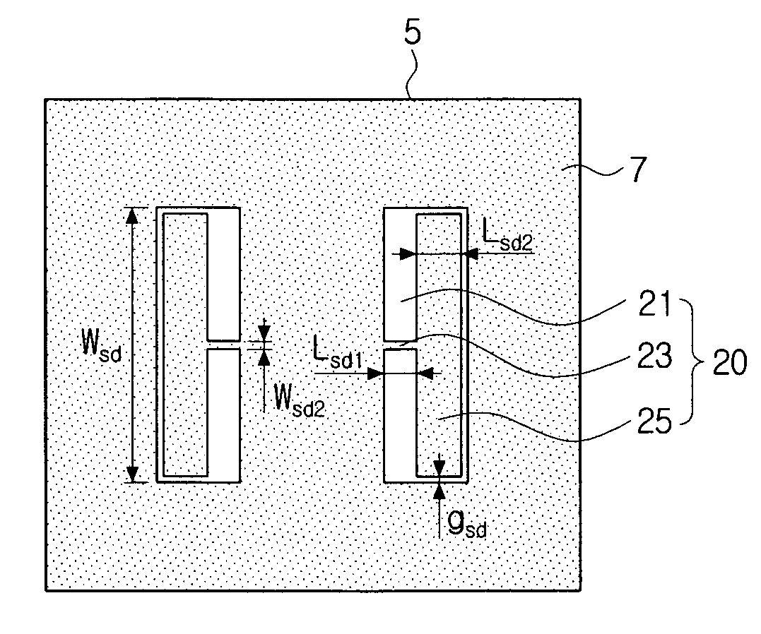
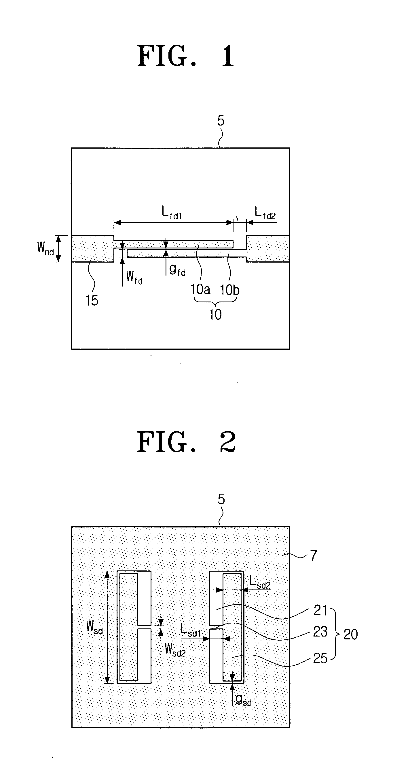
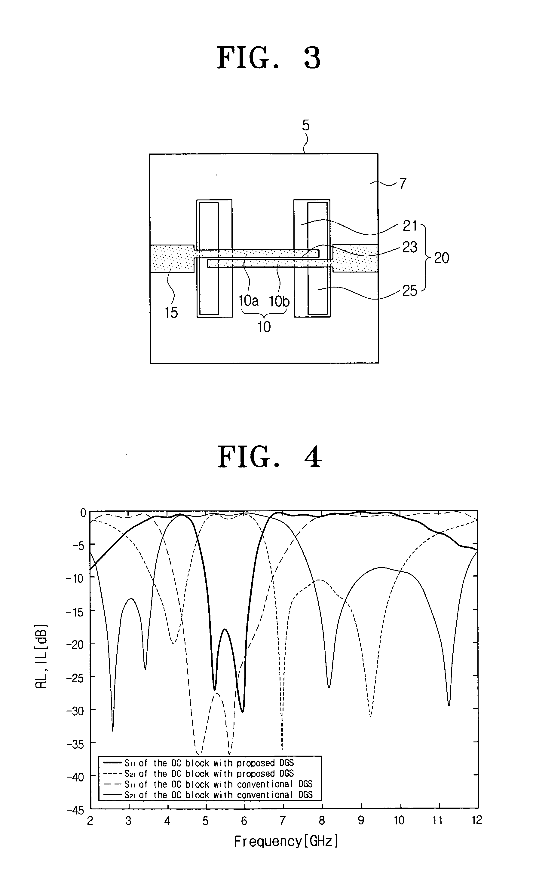
[0037]FIG. 1 is a plane view showing coupled lines for a DC block used in a general active circuit according to an exemplary embodiment of the present invention, and FIG. 2 is a plane view showing a DGS formed corresponding to the coupled lines for a DC block according to an exemplary embodiment of the present invention. The coupled lines for a DC block are formed on one surface of a dielectric 5, and the DGS 20 is formed on the rear surface of the dielectric 5.

[0038] The coupled lines 10 for a DC block are formed at ends of an active circuit to mutually block a signal line 15 and the active circuit, so that the coupled lines 10 for a DC block can function as an open circuit for the DC. Accordingly, the DC power supplied to the active circuit and the signal transmitted through the signal line 15 can be separated.

[0039] Each of the coupl...


PUM


Abstract

A DC block with a band-notch characteristic using a defected ground structure (DGS), includes a pair of coupled lines for being formed parallel to each other on one surface of a dielectric and blocking a flow of a DC, and at least one DGS for being formed on an area of the rear surface of the dielectric corresponding to each coupled line and comprising an etched region formed by etching a part of a ground surface bonded to the dielectric and a metal region formed in the etched region. Accordingly, the stop band of the desired bandwidth in the desired communications band can be formed and the size of the communications system can be reduced.

Description

CROSS-REFERENCE TO RELATED APPLICATIONS [0001] This application claims priority from Korean Patent Application No. 10-2006-0010864, filed Feb. 3, 2006 in the Korean Intellectual Property Office, the entire contents of which are incorporated herein by reference. BACKGROUND OF THE INVENTION [0002] 1. Field of the Invention [0003] The present invention relates to a direct current (DC) block with a band-notch characteristic using a DGS. More particularly, the present invention relates to a DC block with a band-notch characteristic using a defected ground structure (DGS) to superiorly block a certain frequency band in the UWB. [0004] 2. Description of the Related Art [0005] In general, the ultra wideband (UWB) communications can perform high-speed data transmission in a very wide frequency band with a very low power. The frequency band used for the UWB communications is 3.1 ˜ 10.6 GHz, and 5.15˜5.825 GHz of that range is used for HIPERLAN / 2 or Institute of Electrical and Electronics Engi...

Claims


Application Information

Patent Timeline
IPC IPC(8): H01P1/203
CPCH01P1/2007H01P5/04
Inventor YOON, ICK-JAELEE, SEONGSOOYOON, YOUNG JOONGKIM, YOUNG-HWANKIM, YOUNG-EILKIM, HYUNGRAK
Owner SAMSUNG ELECTRONICS CO LTD
Why Eureka
Try Eureka