
Organic thin-film transistor and fabrication method thereof and organic thin-film device

a thin-film transistor and organic technology, applied in transistors, solid-state devices, thermoelectric devices, etc., can solve the problem of difficulty in obtaining an organic tft of n-type having a high electron-mobility, and achieve the effect of higher carrier-mobility

Active Publication Date: 2007-08-23
KANTO DENKA IND CO LTD
View PDF6 Cites 10 Cited by
  • Summary
  • Abstract
  • Description
  • Claims
  • Application Information

AI Technical Summary

Benefits of technology

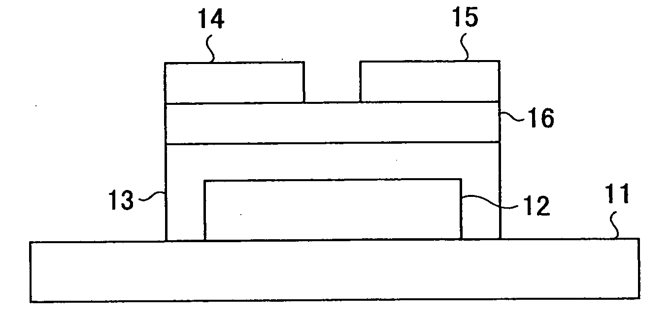
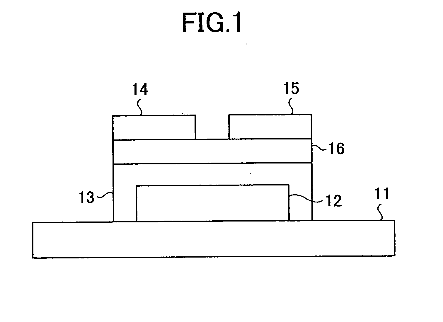
[0011] According to the first aspect of the present invention, an organic thin-film transistor having a higher carrier-mobility can be provided since the organic semiconductor layer contains a fluorinated acene compound which is represented by a formula of C4n+2F2n+4, wherein n is an integer of 2 or greater.
[0030] According to the present invention, an organic thin-film transistor having a higher carrier-mobility, a method of fabricating the organic thin-film transistor and an organic thin-film device including the organic thin-film transistor can be provided.

Problems solved by technology

However, it is difficult to obtain an n-type organic TFT having a high electron-mobility compared to an electron-mobility of amorphous silicon using these materials (for example, see Z. Bao et al., J. Am. Chem., Soc., Vol. 120, pp.

Method used


Image

  • Organic thin-film transistor and fabrication method thereof and organic thin-film device
  • Organic thin-film transistor and fabrication method thereof and organic thin-film device
  • Organic thin-film transistor and fabrication method thereof and organic thin-film device

Examples


example 1

PRACTICAL EXAMPLE 1

[0082] {1} Synthesis of tetradecafluoropentacene

[0083] First, tetradecafluoropentacene was synthesized by the following procedures.

[0084] {1-1} First, 1,2,3,4,8,9,10,11-octafluoro-5,7,12,14-tetrahydroxypentacene-6,13-dione (3) was synthesized from 5,6,7,8-tetrafluoro-9,10-dihydroxy-2,3-dihydroanthracene-1,4-dione (1) and 4,5,6,7-tetrafluoroisobenzofuran-1,3-dione (2).

[0085] 5,6,7,8-tetrafluoro-9,10-dihydroxy-2,3-dihydroanthracene-1,4-dione (1) (9.84 g, 31.3 mmol), 4,5,6,7-tetrafluoroisobenzofuran-1,3-dione (2) (5.75 g, 26.1 mmol), aluminum chloride (1.53 g, 11.5 mmol), and sodium chloride (10.0 g, 171 mmol) were thrown into a 200 mL autoclave made of SUS and heating was made at 280° C. for 1 hour. After the completion of the reaction, cooling was made down to room temperature, the reaction mixture was poured into dilute hydrochloric acid, and stirring was made at 100° C. for 1 hour. Subsequently, the mixture was filtered and the residue was washed with methanol...

example 2

PRACTICAL EXAMPLE 2

[0115] {1} Synthesis of dodecafluoronaphthacene

[0116] First, dodecafluoronaphthacene was synthesized by the following procedures.

[0117] {1-1} First, 1,2,3,4,7,8,9,10-octafluoro-6,11-tetrahydroxynaphthacene-5,12-dione (7) was synthesized from 1,2,3,4-tetrafluoro-5,8-dimethoxynaphthalene (6) and 4,5,6,7-tetrafluoroisobenzofuran-1,3-dione (2).

[0118] 1,2,3,4-tetrafluoro-5,8-dimethoxynaphthalene (6) (4.77 g, 18.3 mmol), 4,5,6,7-tetrafluoroisobenzofuran-1,3-dione (2) (4.77 g, 21.7 mmol), aluminum chloride (23.1 g, 173 mmol), and sodium chloride (3.56 g, 60.9 mmol) were thrown into a 200 mL autoclave and heating was made at 200° C. for 1 hour. After the completion of the reaction, cooling was made down to room temperature, the reaction mixture was poured into dilute hydrochloric acid, and stirring was made at 100° C. for 1 hour. Subsequently, the mixture was filtered and the residue was washed with water, methanol and ether in order. The obtained solid was recrystalli...


PUM


Abstract

An organic thin-film transistor having a higher carrier-mobility, a method of fabricating the organic thin-film transistor and an organic thin-film device including the organic thin-film transistor are provided. In an organic thin-film transistor having an organic semiconductor layer, the organic semiconductor layer contains a fluorinated acene compound which is represented by a formula of C4n+2F2n+4, wherein n is an integer of 2 or greater. The fluorinated acene compound is preferably tetradecafluoropentacene or dodecafluoronaphthacene.

Description

TECHNICAL FIELD [0001] The present invention relates to an organic thin-film transistor and a method of fabricating an organic thin-film transistor and an organic thin-film device. BACKGROUND ART [0002] In recent years, a study or development for utilizing an organic compound as a semiconductor material has been actively conducted and a study intended for utilizing a material of organic compound instead of a conventional device based on silicon is also being paid attention to in the field of a thin-film transistor (Thin Film Transistor; TFT), which has been frequently used for a logic element or a switching element. Since it is easier to process an organic compound compared to silicon as an inorganic substance, it is expected that a low-cost device can be realized by utilizing an organic compound as a semiconductor material. Also, a variety of substrates, which include a plastic substrate, can be used in regard to a semiconductor device utilizing an organic compound, since it is pos...

Claims


Application Information

Patent Timeline
Patent Type & Authority Applications(United States)
IPC IPC(8): H01L29/08H01L21/336H01L21/363H01L29/786H10K99/00
CPCH01L51/0545H01L51/0055H10K85/623H10K10/466H10K71/164H10K85/615
Inventor INOUE, YOUJITOKITO, SHIZUOKOBAYASHI, MASAFUMIGAO, YUAN
Owner KANTO DENKA IND CO LTD
Learn More