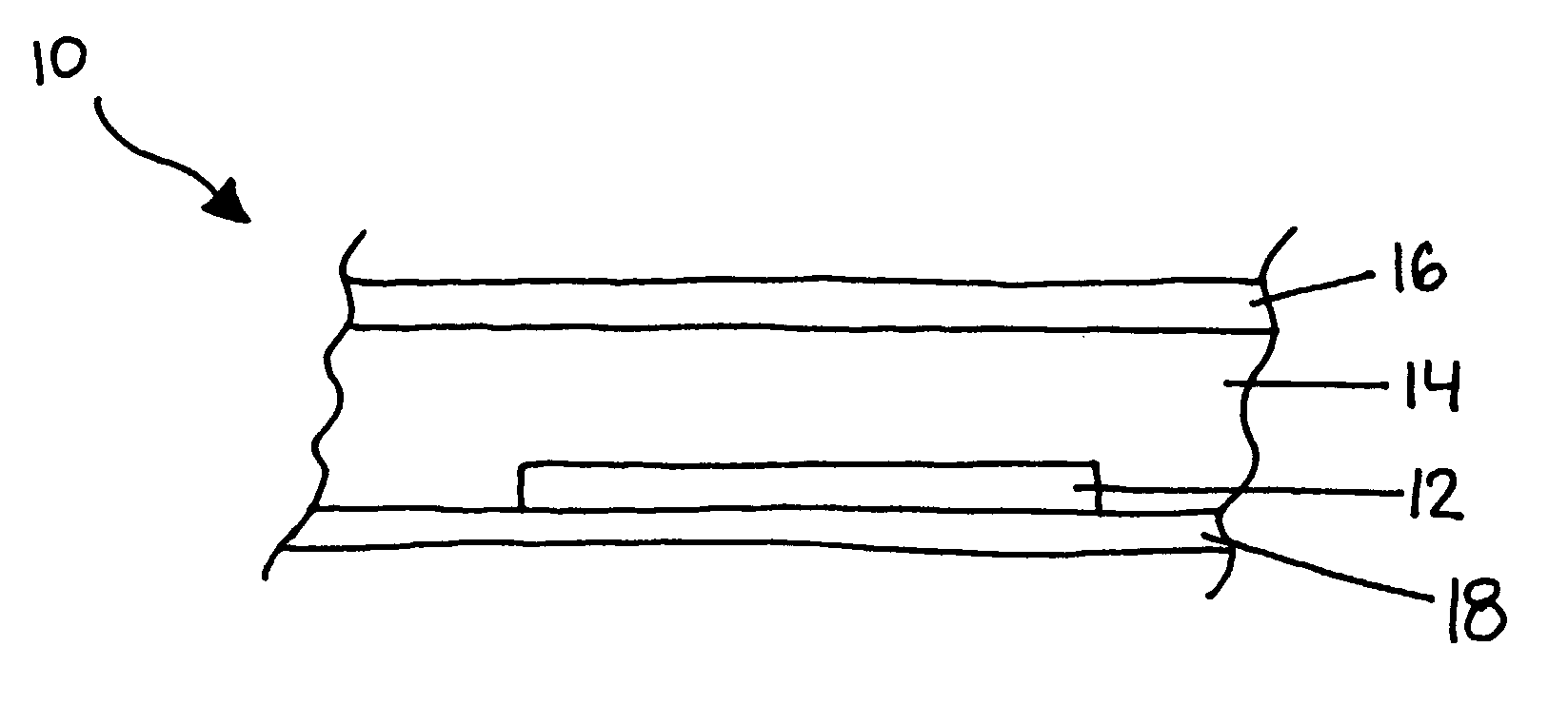
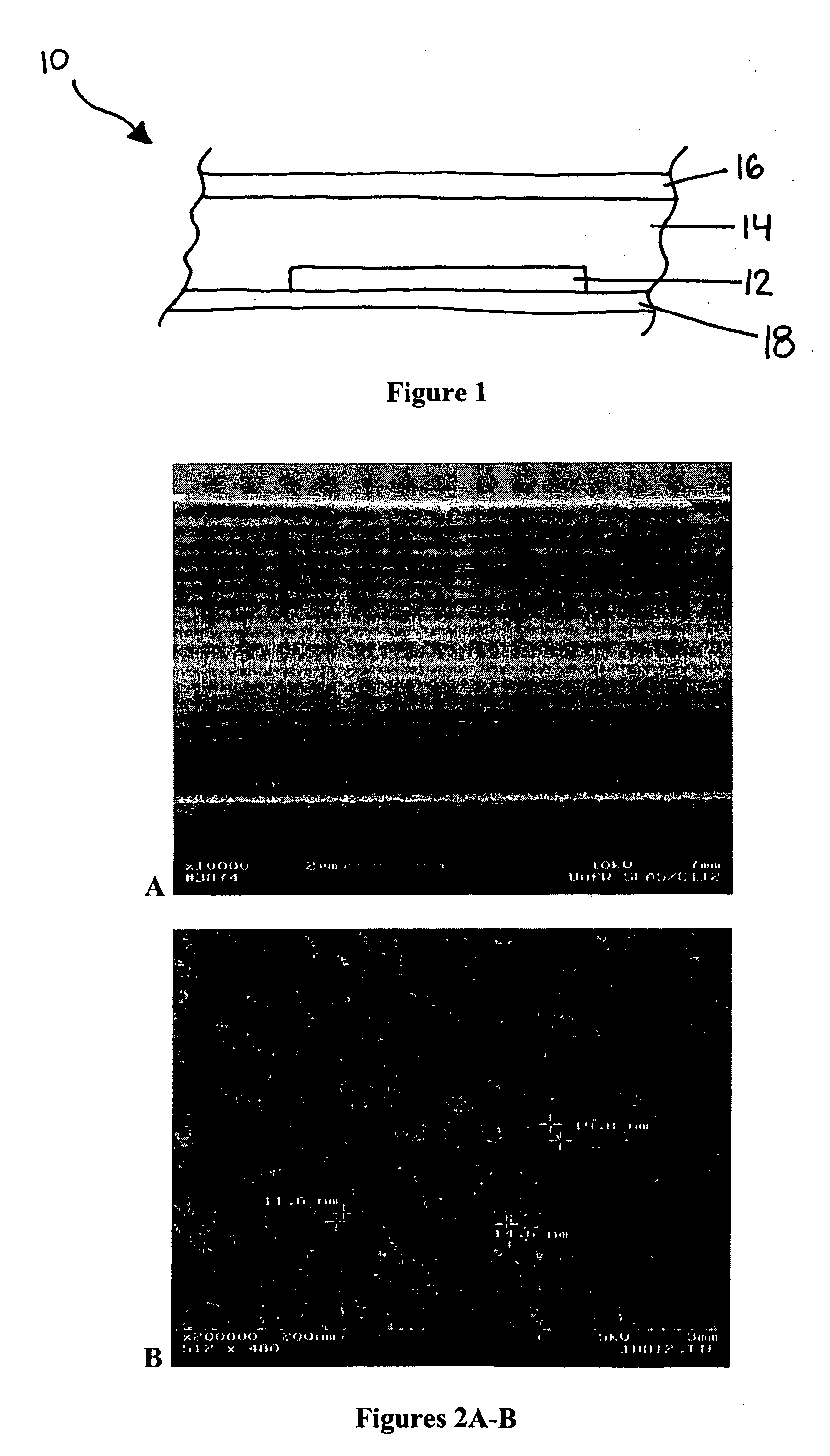
Hydrogel-supported porous semiconductor devices
a technology of porous semiconductors and hydrogels, applied in bandages, instruments, diagnostic recording/measuring, etc., can solve the problems of limiting device function, unable to meet challenges in part, and no noninvasive means of detection, so as to improve treatment efficiency, improve treatment efficiency, and improve treatment
- Summary
- Abstract
- Description
- Claims
- Application Information
AI Technical Summary
Benefits of technology
Problems solved by technology
Method used
Image

Examples
example 1
on of Porous Semiconductor Material
[0063] Details of exemplary mesoporous silicon λ / 2 microcavity fabrication methods are described in, e.g., Vinegoni et al., in Nalwa, ed., Silicon Based Materials and Devices: Properties and Devices, Vol. 2, Academic Press, pg. 124 (2001), and DeLouise & Miller, Proc. SPIE, 5357:111 (2004), each of which is hereby incorporated by reference in its entirety. Briefly, a multilayer microcavity was fabricated by anodic electrochemical etching of a p+ silicon wafer using an ethanolic 14% HF electrolyte. A constant current density was applied for a fixed time and cycled between different current densities to produce a multilayer device with different porosity layers. A current density of 20 mA / cm2 at an etch rate of ˜18 nm / sec produces a low porosity layer of ˜65%. A current density of 70 mA / cm2 at an etch rate of ˜37 nm / sec produces a higher porosity layer of ˜85%. Each mirror used in this Example contains 9 periods of high and low porosity layers. Poro...
example 2
ydrogel-Supported Porous Semiconductor Material
[0066] Hydrogel-supported porous semiconductor material sensors were prepared by either laminating the released porous semiconductor material directly onto pre-cross-linked gel or by pouring an activated solution of monomer over the microcavity prior to the onset of cross-linking. Synthetic (polyacrylamide, polyvinyl pyrrolidone) and natural (agarose) hydrogels and their mixtures were used.
[0067] Alternatively, the released porous semiconductor material was laminated onto pre-cross-linked commercially available wound care products, for example NU-GEL® Wound Dressing sheet (Johnson and Johnson) (“NU-GEL® sheet”), NU-GEL® Collagen Wound Gel (Johnson and Johnson) (“NU-GEL®Gel”), 3M™ Tegaderm™ Absorbent Clear Acrylic Dressing (3M), and ClearSite® TM Transparent Membrane sheet (ConMed). Commercial bandages offer a unique advantage in that they are typically packaged in a semi-dehydrated state and they are engineered with tack on the gel-mat...
example 3
f Optical Response, Stability, and Sensitivity of the Hydrogel-Supported Porous Semiconductor Material
[0069] A porous semiconductor material (˜5.2 μm thick) was constructed from p+ silicon with 9 periods per mirror of a high porosity (85%) and low porosity (˜65%), tuned to operate in the visible spectrum with a resonance dip at 725 nm, and transferred by contact lamination to a NU-GEL® sheet, shown in FIG. 5.
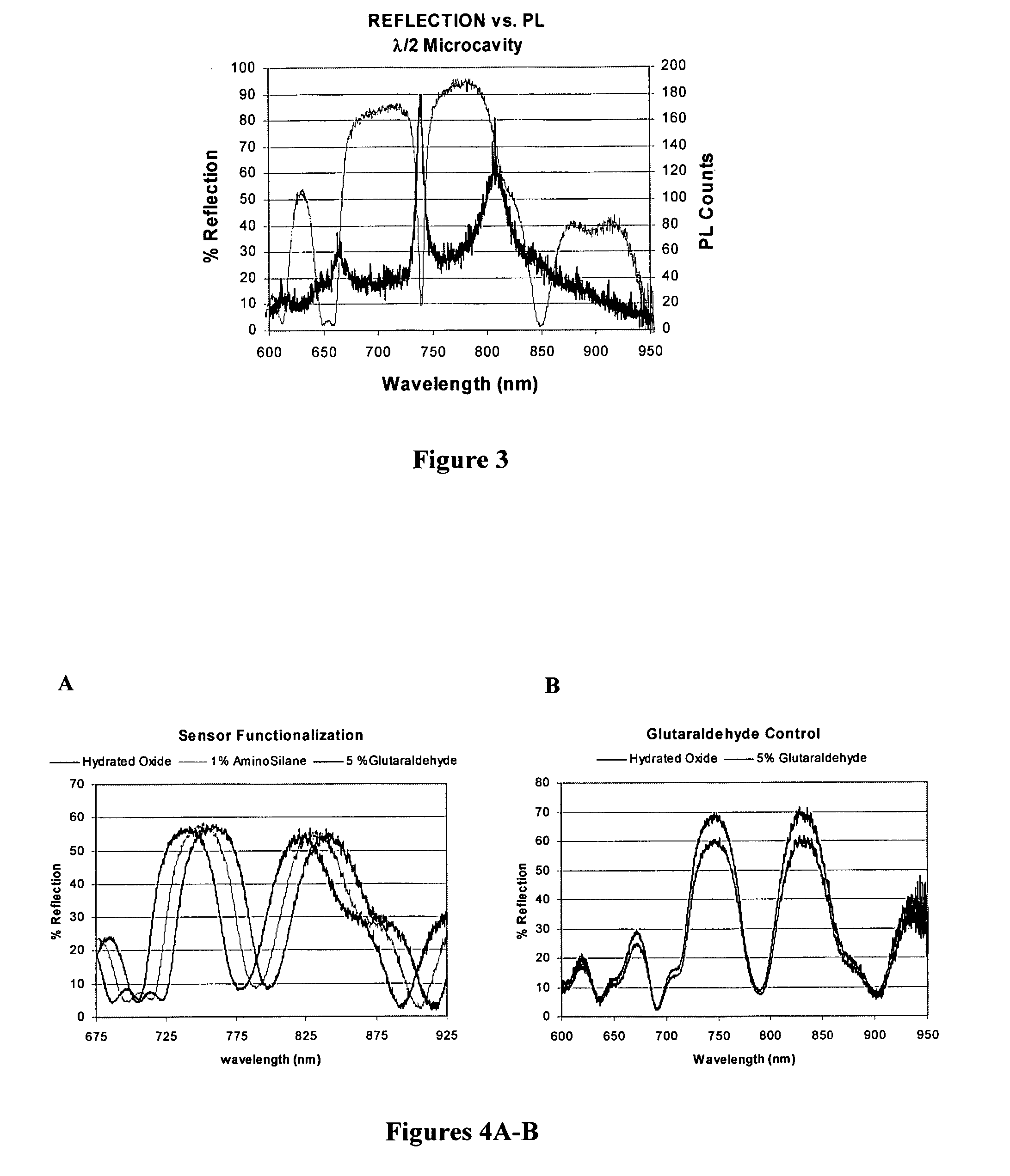
[0070] The optical response before transfer, immediately after transfer, 3 days after transfer, and 1 year following transfer is shown in FIG. 6. The porous semiconductor material resonance undergoes a large red wavelength shift of ˜150 nm resulting from transfer to the hydrogel. The magnitude of the red shift is consistent with optical simulations in which air in the pores is displaced 100% with water (η=1.33) (see DeLouise & Miller., Proc. SPIE, 5357:111 (2004), which is hereby incorporated by reference in its entirety). FIG. 6 also demonstrates how remarkably stable the sens...
PUM
| Property | Measurement | Unit |
|---|---|---|
| thick | aaaaa | aaaaa |
| thick | aaaaa | aaaaa |
| thick | aaaaa | aaaaa |
Abstract
Description
Claims
Application Information
 - R&D
- Intellectual Property
- Life Sciences
- Materials
- Tech Scout
- Unparalleled Data Quality
- Higher Quality Content
- 60% Fewer Hallucinations
Browse by: Latest US Patents, China's latest patents, Technical Efficacy Thesaurus, Application Domain, Technology Topic, Popular Technical Reports.
© 2025 PatSnap. All rights reserved.Legal|Privacy policy|Modern Slavery Act Transparency Statement|Sitemap|About US| Contact US: help@patsnap.com