
Semiconductor device and method of forming the same

a semiconductor and semiconductor technology, applied in the direction of semiconductor devices, electrical equipment, transistors, etc., can solve the problems of less space for a smaller chip, disadvantages in current capacity and cost, and chip disadvantages at electrical characteristics and cost, and achieve no improvement of area in the described structur

Inactive Publication Date: 2007-08-02
FUJI ELECTRIC HLDG CO LTD
View PDF5 Cites 18 Cited by
  • Summary
  • Abstract
  • Description
  • Claims
  • Application Information

AI Technical Summary

Benefits of technology

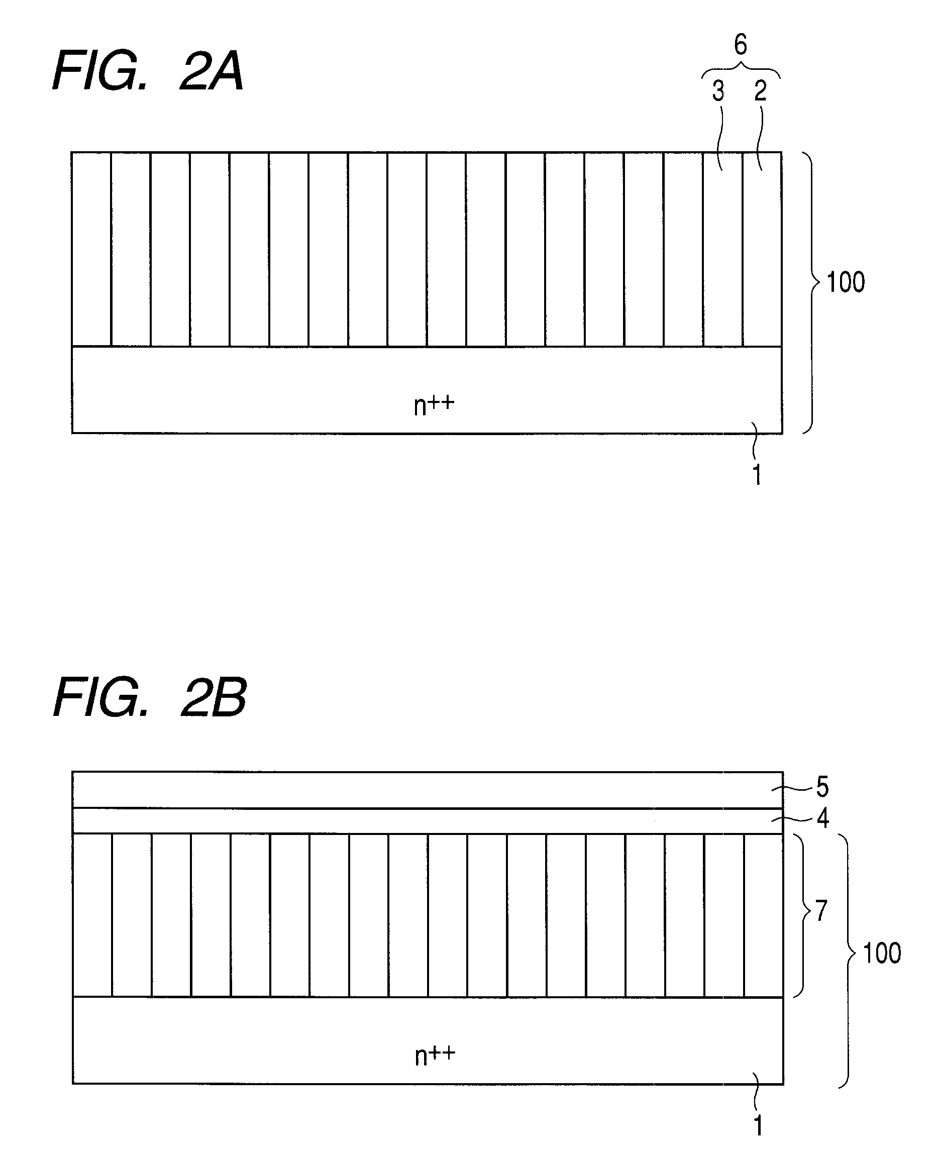
[0016]The semiconductor device can be a MOSFET, a diode, or an IGBT. The drift layer can have a superjunction structure including pin stripe regions of the first conductivity type and pin stripe isolating regions of the second conductivity type perpendicular to the principal surface of the first high impurity concentration layer and arranged alternately, adjacently, and parallel with each other.
[0017]Another aspect of the prese

Problems solved by technology

Therefore, particularly in a high breakdown voltage semiconductor substrate (chip), the area ratio of the breakdown voltage blocking structure to the entire area of the chip becomes relatively larger as the area of the chip becomes smaller, which makes the chip disadvantageous at to electrical characteristics and cost.
This, as described before, is more disadvantageous for a smaller area chip in current capacity and as well as in cost.
None of the described structures, however, provides improvements relating to the area ratio of the surface of a breakdown voltage blocking structure to the entire area of a chip.
As a result, the semiconductor device described in JP-A-2005-136064 (FIG. 23) sometimes causes breakdown at a low applied voltage, so that it is hard to ensure a sufficiently high breakdown voltage.

Method used


Image

  • Semiconductor device and method of forming the same
  • Semiconductor device and method of forming the same
  • Semiconductor device and method of forming the same

Examples


Embodiment Construction

[0056]Examples according to the invention will be explained in detail referring to the drawings. The present invention is not to be limited only to the examples provided herein. In the specification and the attached drawings, a leading character “n” or “p” attached to the name of a layer or a region means that majority carriers in the layer or the region are electrons or holes, respectively. Moreover, a sign “+” attached to the leading character “n” or “p” means that the layer or the region has a comparatively high impurity concentration, and a sign “−” attached to the leading character “n” or “p” means that the layer or the region has a comparatively low impurity concentration. Furthermore, a sign “++” means that the layer or the region has a further higher impurity concentration. The n-type and p-type structure can be exchangeably used.

[0057]In Example 1, a superjunction MOSFET with a breakdown voltage of 600 V is picked up and explanations thereon including the manufacturing meth...


PUM


Abstract

A semiconductor device and a method of forming thereof have a semiconductor substrate, an active region, and an inclined trench formed around the outer periphery of the active region. The semiconductor substrate at least includes an n-type high impurity concentration layer inhibiting a depletion layer from spreading, an n-type low impurity concentration drift layer, and a p-type high impurity concentration layer forming a p-n main junction between the drift layer, which are arranged in this order. In the active region, an effective current flows in the direction of the thickness of the substrate. The inclined trench cuts the p-n main junction at a positive bevel angle from the semiconductor substrate surface on the side of the n-type high impurity concentration layer to penetrate through the substrate for separating it into chips. In the semiconductor device, along the sidewall of the inclined trench in the n-type drift layer, an n-type surface region is formed with an impurity concentration lower than that in the n-type drift layer. Thus provided semiconductor device can prevent the electric field strength therein from reaching the critical electric field strength that causes a breakdown in a surface breakdown voltage blocking structure prior to in the active region, as well as reducing the area ratio of the surface breakdown voltage blocking structure to the entire chip area.

Description

BACKGROUND[0001]In a semiconductor device such as a diode, a BJT, a superjunction MOSFET, or an IGBT in which a number of semiconductor devices are formed in a semiconductor wafer, a planar type junction termination structure is mainly used as a breakdown voltage blocking structure of the device. In the planar type junction termination structure, the termination of a p-n junction is made to intersect the principal surface of a semiconductor wafer and the surface of the intersection is coated with a passivation film such as an insulator film for protection.[0002]A planar type breakdown voltage blocking structure is normally arranged around the outer periphery of an active region positioned at the central section of a semiconductor device. The breakdown voltage blocking structure has a junction termination structure including a curved p-n junction face linking to the outer periphery of a planar p-n junction face corresponding to an active region. In the planar type breakdown voltage b...

Claims


Application Information

Patent Timeline
IPC IPC(8): H01L29/76
CPCH01L29/0615H01L29/0634H01L29/0661H01L29/402H01L29/868H01L29/6609H01L29/66712H01L29/7811H01L29/41741
Inventor YOSHIKAWA, KOH
Owner FUJI ELECTRIC HLDG CO LTD
Learn More