
Method of adjusting pattern density

Inactive Publication Date: 2007-07-26
SAMSUNG ELECTRONICS CO LTD
View PDF7 Cites 23 Cited by
  • Summary
  • Abstract
  • Description
  • Claims
  • Application Information

AI Technical Summary

Benefits of technology

[0007]Exemplary embodiments of the present invention provide a method of adjusting a pattern density in a semiconductor device. The method of adjusting a pattern density can minimize distribution of global pattern densities and conduct a process in an optimum condition when a product type is changed.
[0008]The method of adjusting a pattern density may provide a global pattern density for rendering a process conducted under an optimum processing condition.
[0009]The method of adjusting a pattern density may minimize gaps of designed pattern densities over a chip area, thereby providing the optimum global pattern density.

Problems solved by technology

The line widths of circuit patterns may be inconsistent throughout the semiconductor device due to an irregular density of circuit patterns.

Method used


Image

  • Method of adjusting pattern density
  • Method of adjusting pattern density
  • Method of adjusting pattern density

Examples


Embodiment Construction

[0030]Exemplary embodiments of the present invention will be described in more detail with reference to the accompanying drawings. The present invention may, however, be embodied in many different forms and should not be construed as limited to the embodiments set forth herein.

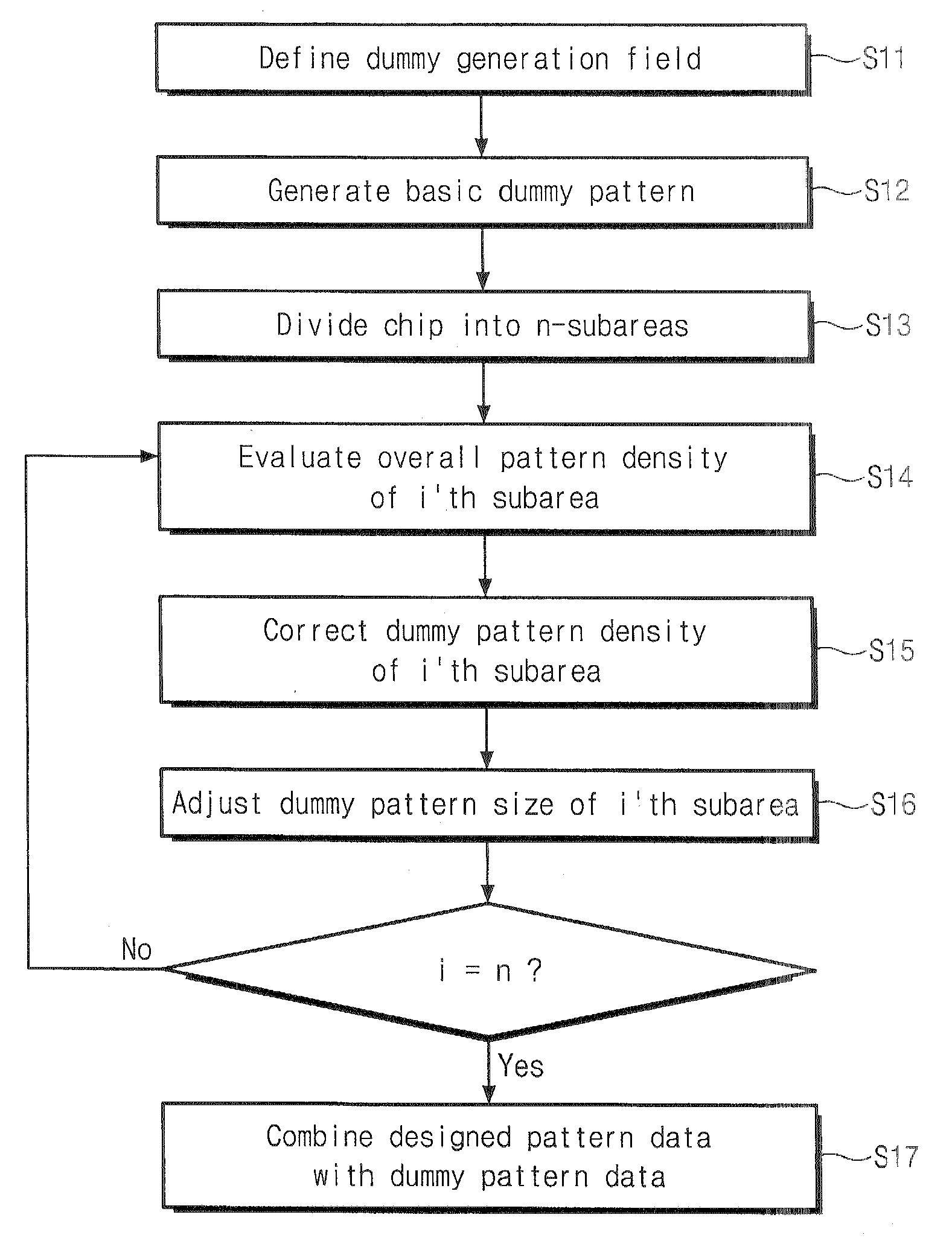
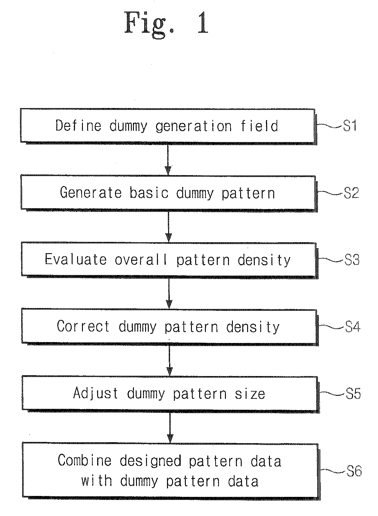
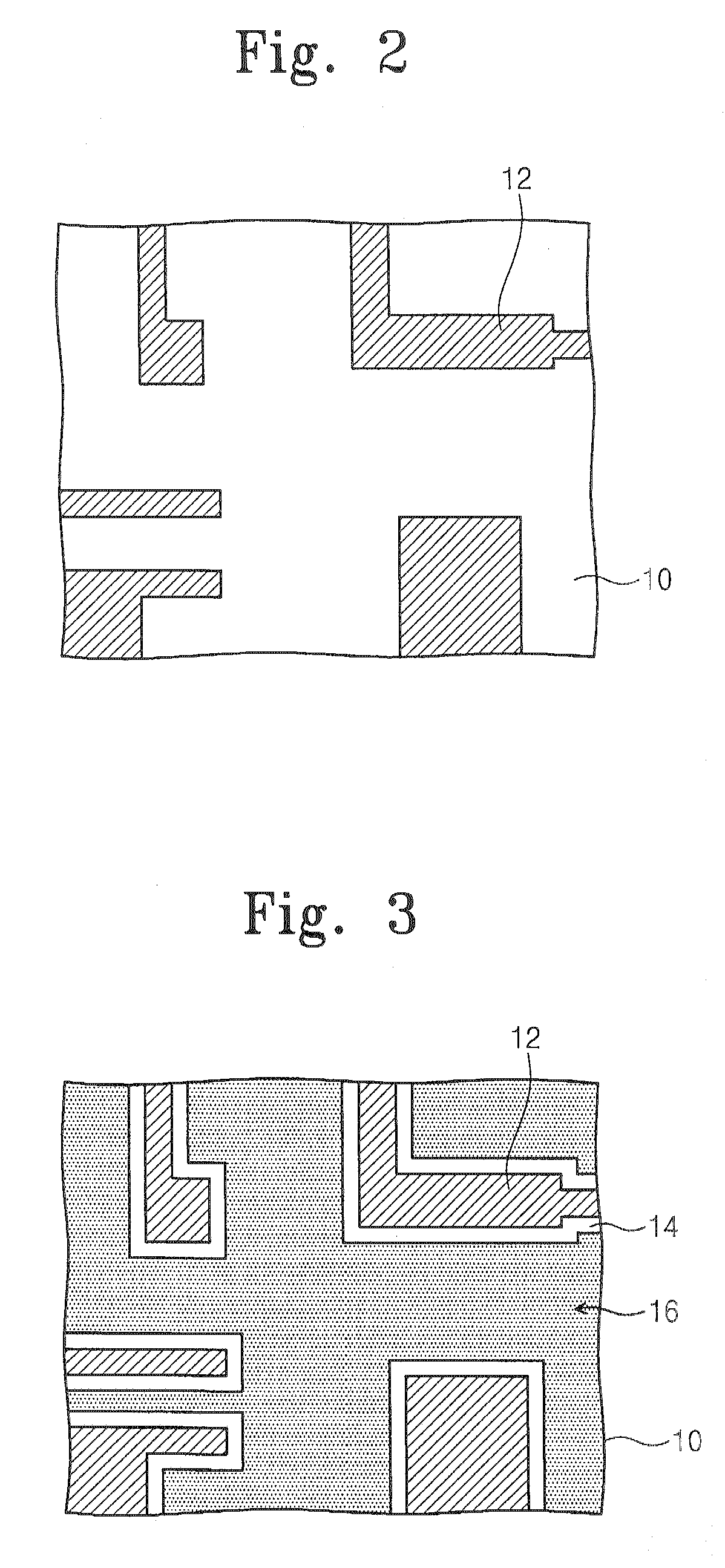
[0031]FIG. 1 is a flow chart showing a method of adjusting a pattern density in accordance with an exemplary embodiment of the present invention. FIGS. 2 through 5 are plan views illustrating a method of adjusting a pattern density according to an exemplary embodiment of the present invention.

[0032]Referring to FIG. 1, step S1 defines a dummy generation field in a chip area. The chip area refers to a virtual chip area provided for a photomask, not an area formed on a wafer. Referring to FIG. 2, designed patterns 12 for constituting circuits are arranged in a virtual chip area 10. The designed patterns 12 are disposed in accordance with predetermined data for a circuit design. Referring to FIG. 3, dummy generat...


PUM


Abstract

A method of adjusting pattern density includes determining a reference pattern density, defining dummy generation fields and designed patterns, forming basic dummy patterns on the dummy generation fields, evaluating a total pattern density from a sum of a density of the designed patterns and a density of the basic dummy patterns, adjusting a size of the basic dummy patterns so that the total pattern density reaches the reference pattern density, and combining data of the adjusted dummy patterns with data of the designed patterns.

Description

CROSS-REFERENCE TO RELATED APPLICATION[0001]This application claims priority under 35 U.S.C. §119 to Korean Patent Application No. 2006-006882, filed on Jan. 23, 2006, the disclosure of which is incorporated herein by reference in its entirety.BACKGROUND[0002]1. Technical Field[0003]The present disclosure relates to a method of adjusting a pattern density in a semiconductor device, and more particularly to a method of adjusting a pattern density in a semiconductor device for minimizing pattern deformation.[0004]2. Discussion of Related Art[0005]In fabricating a semiconductor device, operational characteristics of electronic circuits can be affected by the line widths of circuit patterns,. The line widths of circuit patterns are determined by photolithography and etching processes during the manufacture of a semiconductor device. The line widths of circuit patterns may be inconsistent throughout the semiconductor device due to an irregular density of circuit patterns. For instance, w...

Claims


Application Information

Patent Timeline
IPC IPC(8): G06F17/50
CPCG03F1/36G03F1/144G03F1/80
Inventor SHIN, JAE-PILYOO, MOON-HYUNLEE, JONG-BAECHOI, JIN-SOOKPARK, SUNG GYU
Owner SAMSUNG ELECTRONICS CO LTD
Learn More