Method of making electronic device with frit seal and frit sealing apparatus

a technology of electronic devices and sealing apparatus, which is applied in the field of packaging of organic light-emitting display devices, can solve the problems of increasing material and process costs, increasing the thickness of the display device, and being vulnerable to oxygen degradation in the presence of oxygen

Inactive Publication Date: 2007-07-26
SAMSUNG DISPLAY CO LTD
View PDF10 Cites 32 Cited by
  • Summary
  • Abstract
  • Description
  • Claims
  • Application Information

AI Technical Summary

Benefits of technology

[0015]Still referring to the above described method, the first substrate may be a single layer substrate. The first substrate may comprise two or more layers of different materials. The radiation source comprises a laser or an infrared lamp. The unfinished device may comprise a plurality of additional arrays of organic light emitting pixels and a plurality of additional frits, which are interposed between the first and second substrates, one of the additional frits surrounding one of the additional arrays, and wherein the mask comprises a plurality of additional transmitting windows, one of the additional transmitting windows is located so as to pass the ray toward one of the additional frits. The method may further include, after directing the ray to the frit, moving the unfinished device relative to the radiation source such that the ray from the radiation source can be directed to the one of the additional transmitting windows. The method may further include, after moving the unfinished device, directing the ray to the one of the additional frits through the one of the additional transmitting windows. The method may further include cutting the resulting product into a plurality of pieces to provide an electronic device comprising a piece of the first substrate, a piece of the second substrate, one array of organic light emitting pixels interposed between the pieces and one frit bonded to and interposed between the pieces while surrounding the one array.

Problems solved by technology

Since the organic light-emitting diode includes organic material, it is vulnerable to degradation in the presence of oxygen.
Further, since the cathode electrode is made of metal material, it may be oxidized by moisture in the air so as to degrade its electrical characteristic and light-emitting characteristics.
However, the method of mounting the moisture absorbent material in the form of powder can cause problems such as complicating the process, increasing material and process costs, increasing the thickness of a display device, and being difficult to apply to a top emitting (front light-emitting) display configuration.
Also, the method of adhering moisture absorbent material in the form of a film can cause problems in that it is limited in its ability to remove moisture and it is difficult to apply to mass production due to low durability and reliability.
However, when the substrate is inserted into the chamber, since heat is transferred to the overall area of the substrate, the thin film transistor and the organic light-emitting diode formed on the substrate are at risk of being damaged.

Method used


Image

  • Method of making electronic device with frit seal and frit sealing apparatus
  • Method of making electronic device with frit seal and frit sealing apparatus
  • Method of making electronic device with frit seal and frit sealing apparatus

Examples


Embodiment Construction

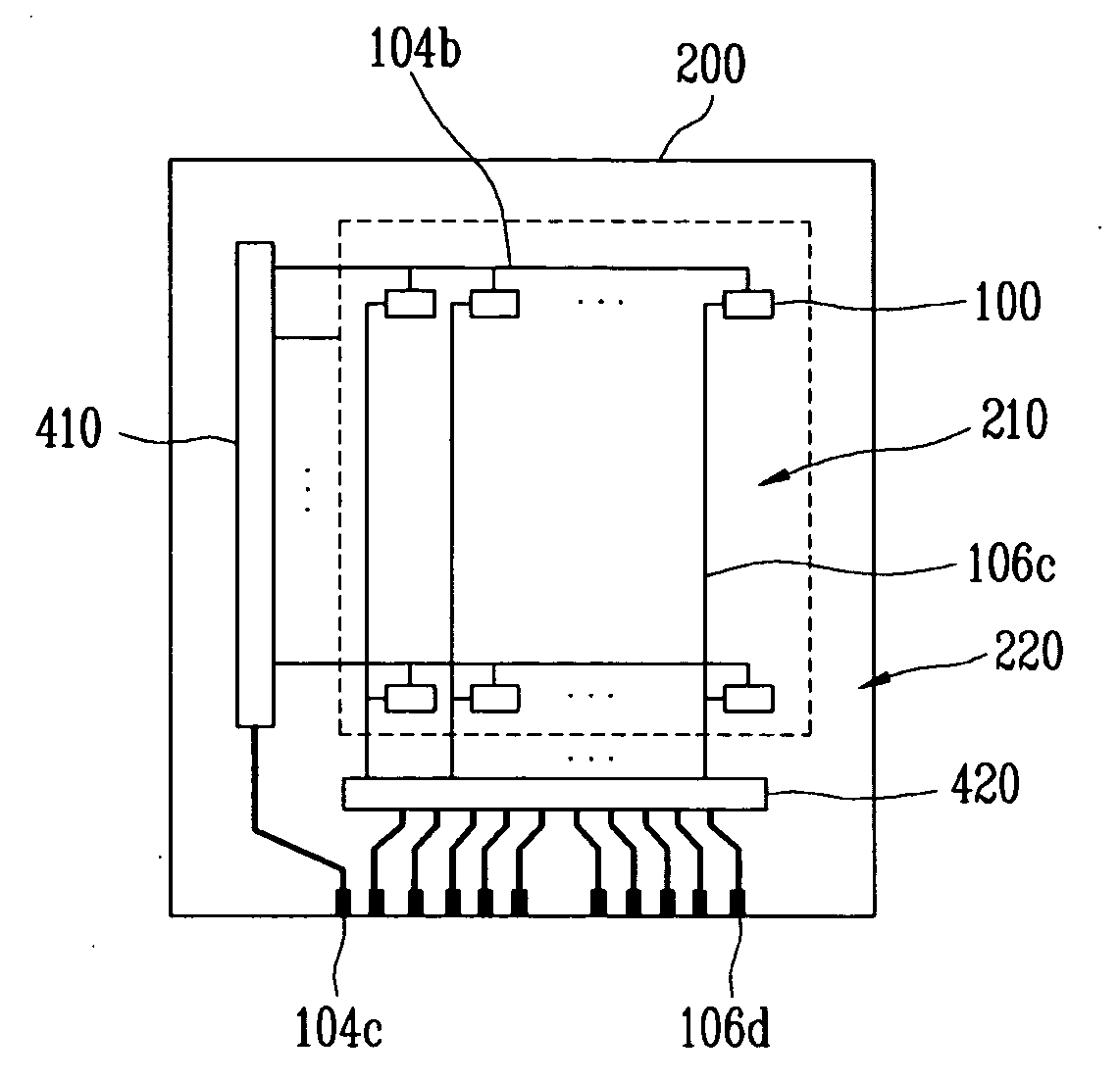
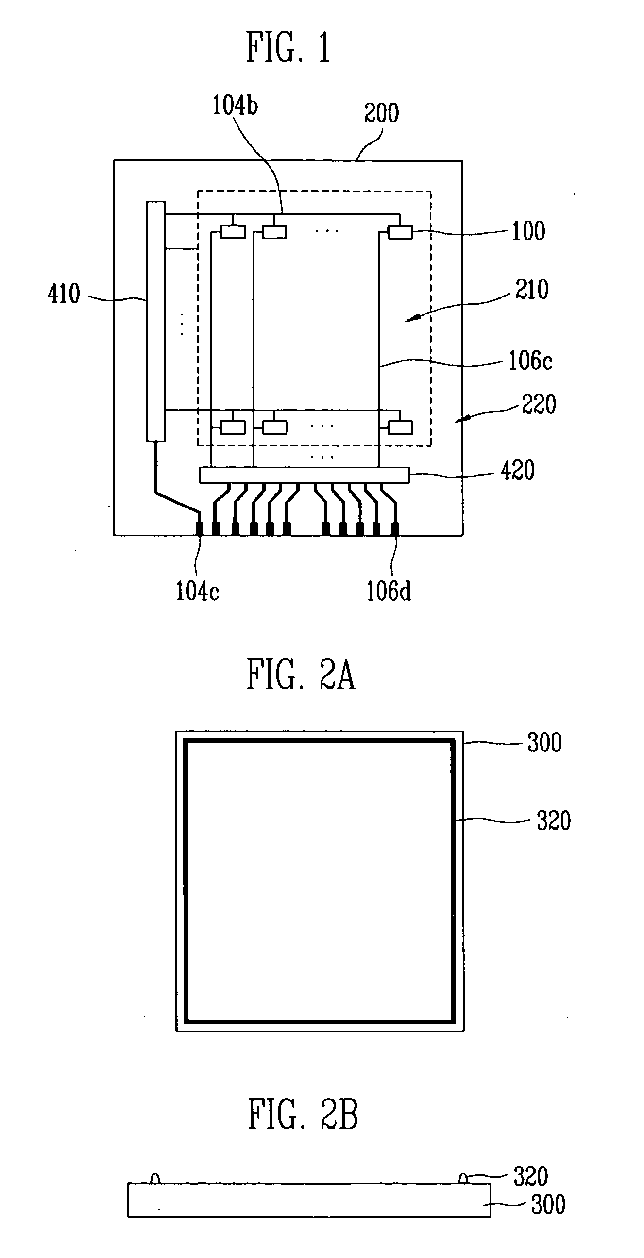
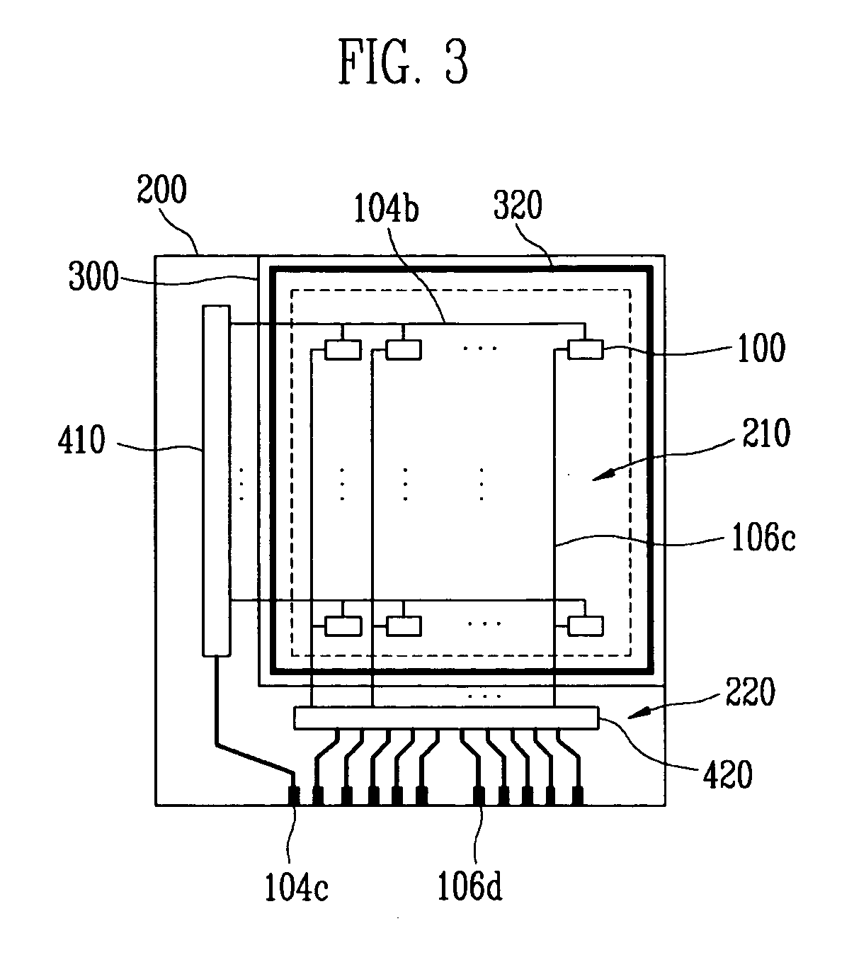
[0028]Embodiments of the present invention will be described with reference to the accompanying drawings. Herein, when one element is described as being connected to another element, one element may be not only directly connected to another element but may also be indirectly connected to another element via yet another element. Further, irrelevant elements are omitted for clarity. Also, like reference numerals refer to like elements throughout.

[0029]An organic light emitting display (OLED) is a display device comprising an array of organic light emitting diodes. Organic light emitting diodes are solid state devices which include an organic material and are adapted to generate and emit light when appropriate electrical potentials are applied.

[0030]OLEDs can be generally grouped into two basic types dependent on the arrangement with which the stimulating electrical current is provided. FIG. 7A schematically illustrates an exploded view of a simplified structure of a passive matrix typ...


PUM

PropertyMeasurementUnit
widthaaaaaaaaaa
widthaaaaaaaaaa
heightaaaaaaaaaa

Abstract

Disclosed is a frit sealing apparatus and method of using the same, the apparatus being capable of irradiating infrared rays only to a frit portion of a substrate. The apparatus includes a first chamber, a second chamber positioned inside the first chamber, a lamp positioned inside the second chamber, a stage positioned outside the first chamber to receive and fix a first mother substrate and a second mother substrate, an emitting part formed in the first chamber and the second chamber and positioned to direct heat supplied by the lamp to the stage. The apparatus also includes a mask positioned over the substrates, the mask including one or more transmitting portions positioned over regions containing the frit, and one or more interrupting portions positioned at other regions.

Description

CROSS-REFERENCE TO RELATED APPLICATIONS[0001]This application claims the benefit of Korean Patent Application No. 2006-08457, filed on Jan. 26, 2006, in the Korean Intellectual Property Office, the disclosure of which is incorporated herein by reference in its entirety.BACKGROUND OF THE INVENTION[0002]1. Field of the Invention[0003]The present invention relates to organic light-emitting display devices. More particularly, the invention relates to packaging of organic light-emitting display devices.[0004]2. Description of the Related Art[0005]In general, an organic light-emitting display device comprises a first substrate comprising a pixel region and a non-pixel region and a second substrate opposed and disposed to the first substrate and bonded to the first substrate with sealant such as epoxy for encapsulation.[0006]In the pixel region of the first substrate a plurality of organic light-emitting diodes are formed at intersecting portions of scan lines and data lines in the form of...

Claims


Application Information

Patent Timeline
Patent Type & Authority Applications(United States)
IPC IPC(8): H01J1/62H01J63/04G09F9/00H01L27/32H05B33/04
CPCB23K26/206B23K26/246H01L51/56B23K2201/40H01L51/5237B23K26/324B23K26/244B23K2101/40H10K59/12H10K71/421H10K59/8722F24C15/14F24C15/006F24C3/085H10K50/8426H10K71/00
Inventor CHA, YOU MIN
Owner SAMSUNG DISPLAY CO LTD
Why Eureka
Try Eureka