
Method for designing a semiconductor device capable of reflecting a time delay effect for dummy metal fill

a technology of time delay and semiconductor devices, applied in the direction of individual semiconductor device testing, semiconductor/solid-state device testing/measurement, instruments, etc., can solve the problems of large-scale integration design (vlsi) of digital circuits, the design complexity of semiconductor devices has been relatively increased, and the line width has been rapidly reduced.

Inactive Publication Date: 2007-06-28
DONGBU ELECTRONICS CO LTD
View PDF4 Cites 27 Cited by
  • Summary
  • Abstract
  • Description
  • Claims
  • Application Information

AI Technical Summary

Benefits of technology

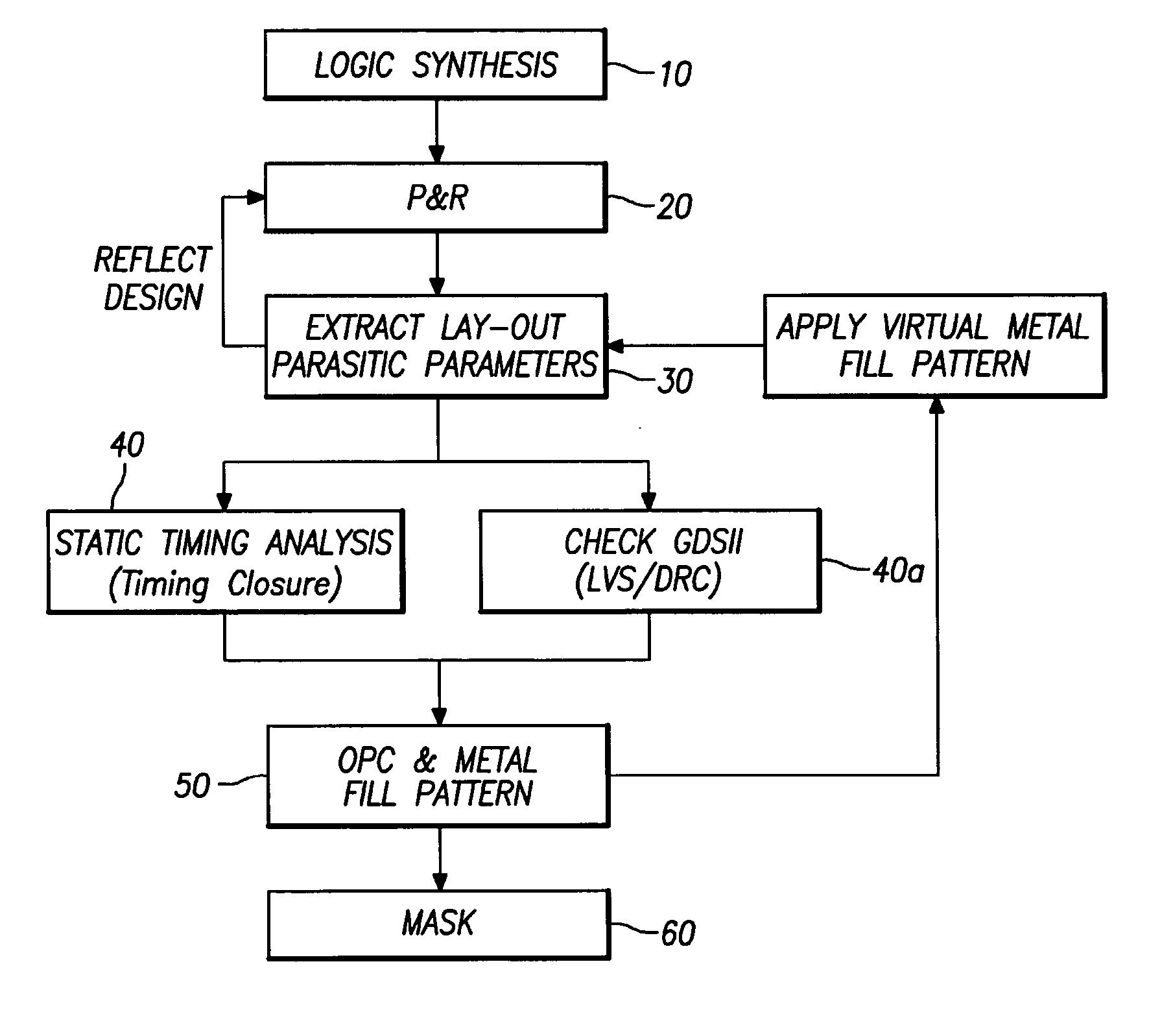
[0020] The present invention has been made to solve the above problems occurring in the prior art. Therefore, consistent with the present invention, there is provided a method for designing a semiconductor device, capable of effectively reflecting a time delay effect caused by dummy metal fill in a design procedure by complementing a disadvantage of an existing semiconductor design scheme which cannot reflect the time delay effect caused by the dummy metal interconnection.
[0021] Further consistent with the present invention, there is provided a method for designing a semiconductor device through logic synthesis, the method comprising a placement and routing step for automatically placing and routing cells having a transistor level; a layout parasitic extract step of extracting a resistor capacitance value of an interconnection between logic elements after the placement and routing step; a static timing analysis step of d

Problems solved by technology

Recently, as semiconductor manufacturing technology has been developed, line width has been rapidly reduced and the design complexity of semiconductor devices has relatively increased.
This is done instead of a circuit having a gate level design, as the complexity of very large-scale integration design (VLSI) for a digital circuit increases, and the demands for a quick time-to-Market increases.
Thus, since the placement & routing is complicated because of placing a great number of cells and connecting the cells to each other, the placement & routing is often performed by computer-aided design (CAD).
However, since this determination is time consuming, only a flip-flop is determined in a logic without inputting an input vector, which is called the static timing analysis (step 40).
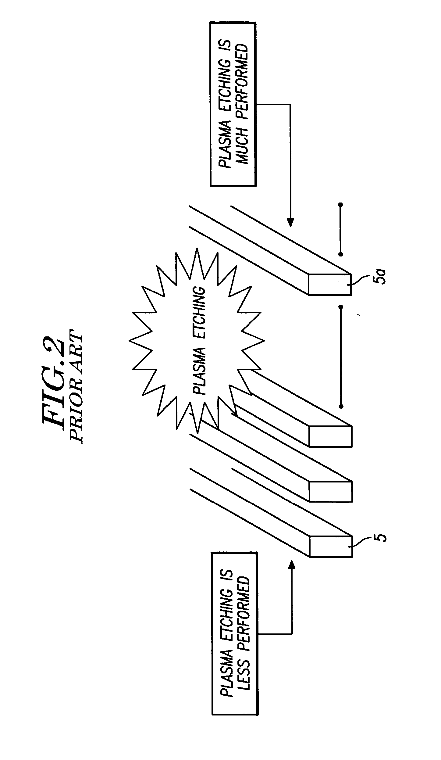
In particular, the reduction of the line width makes a time delay effect resulting from parasitic power capacitance important.
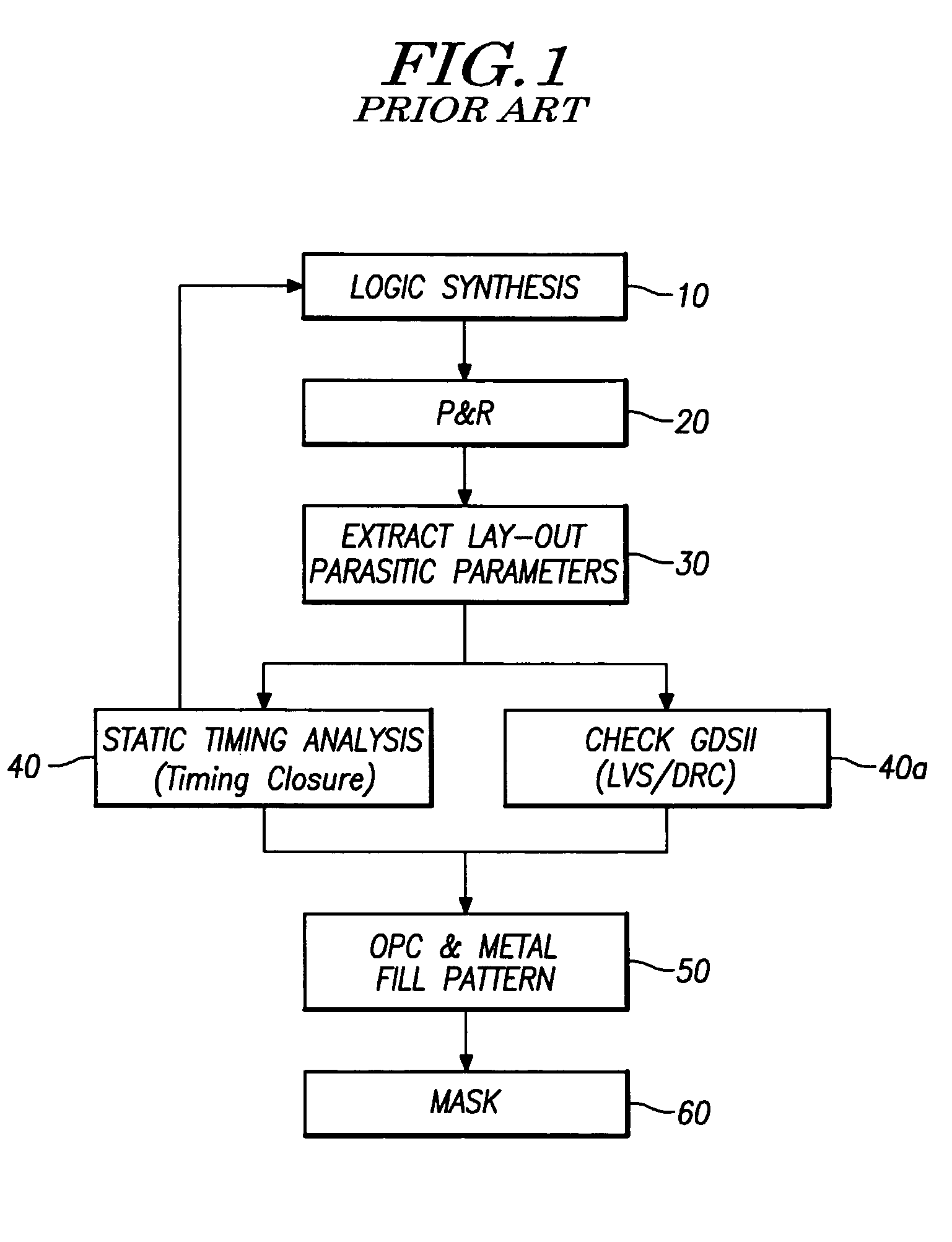
However, as shown in FIG. 1, according to the conventional logic synthesis, since the design of a semiconductor device is completed after the OPC and metal fill pattern forming step, the time delay effect cannot be reflected.
At this time, a problem related to a time delay occurs.
Such problems may degrade the performance and the yield rate of a semiconductor chip as well as functions of the semiconductor chip.
Although only the first metal interconnection layer is shown in FIG. 5, since many metal interconnection layers of the second metal interconnection layer to the eighth metal interconnection layer actually exist, many problems related to time delay occur.
However, in the conventional design of a semiconductor device, it is difficult to take the problems occurring after the completion of semiconductor design into account.

Method used


Image

  • Method for designing a semiconductor device capable of reflecting a time delay effect for dummy metal fill
  • Method for designing a semiconductor device capable of reflecting a time delay effect for dummy metal fill
  • Method for designing a semiconductor device capable of reflecting a time delay effect for dummy metal fill

Examples


embodiment 1

[0029] Hereinafter, a first embodiment consistent with the present invention will be described with reference to the drawings.

[0030] As shown in FIG. 6, a placement & routing (P & R) step (step 20), which is the first step of logic synthesis (see, reference numeral 10) in semiconductor design, automatically places and routes the automatically made logic gates, that is, cells at the transistor level.

[0031] Next, a layout parasitic extract step (step 30), which is the second step of the logic synthesis (see, reference numeral 10), extracts values for resistor capacitance (RC) of an interconnection between logic gates. Since the resistor capacitance value for the interconnection is closely related to a time delay, a resistor capacitance extract value is required in order to completely operate a circuit. To this end, a StarRCXT tool, which is a tool used for extracting resistor capacitance, is used.

[0032] Thereafter, a static timing analysis step (step 40), which is the third step of...

embodiment 2

[0039] Hereinafter, a second embodiment consistent with the present invention will be described with reference to the accompanying drawings.

[0040] As shown in FIG. 7, in a placement & routing (P & R) step (step 20), which is the first step in logic synthesis (see, reference numeral 10), logic gates, that is, cells having a transistor level are placed and routed.

[0041] Next, in a layout parasitic extract step (step 30), which is the second step of the logic synthesis (see, reference numeral 10), values for resistor capacitance (RC) of an interconnection between logic elements are extracted. At this time, a virtual metal-fill pattern is fabricated based on information about an existing metal fill pattern having a defined interval between metal interconnections, and resistor capacitance values are extracted by using the virtual metal-fill pattern. In this case, a StarRCXT tool, which is a tool used for extracting resistor capacitance, is used.

[0042] Thereafter, logic gates, that is,...


PUM


Abstract

Disclosed is a method for designing a semiconductor device. In an existing semiconductor design, a time delay effect caused by a dummy metal interconnection cannot be reflected. In order to address this disadvantage, a real metal fill pattern and a virtual metal fill pattern are employed for a layout parasitic extract step such that a time delay effect caused by the dummy metal pattern in semiconductor design is reflected. Accordingly, a semiconductor device can be designed by effectively reflecting a time delay effect. According to the method, since a real metal fill pattern and a virtual metal fill pattern are employed for a layout parasitic extract step so that resistor capacitance values of interconnections (including dummy interconnections) between logic elements are extracted, it is possible to more exactly design a semiconductor device by tacking a time delay effect into account.

Description

RELATED APPLICATION [0001] This application claims the benefit of Korean Application No. 10-2005-0131445, filed on Dec. 28, 2005, which is incorporated by reference herein in its entirety. BACKGROUND [0002] 1. Technical Field [0003] The present invention relates to semiconductor design technology. More specifically, the present invention relates to a method for designing a semiconductor device capable of effectively reflecting a time delay effect caused by dummy metal fill in a design procedure. [0004] 2. Description of the Related Art [0005] Recently, as semiconductor manufacturing technology has been developed, line width has been rapidly reduced and the design complexity of semiconductor devices has relatively increased. Consequently, integrated circuits with several billion of transistors have been successively developed. [0006] A semiconductor device is designed according to a logic synthesis flowchart shown in FIG. 1. Logic synthesis (see, reference numeral 10) in semiconducto...

Claims


Application Information

Patent Timeline
IPC IPC(8): G06F17/50H01L21/66H01L21/4763G06F9/45G01R31/26
CPCG06F17/505H01L22/20G06F30/327H01L21/02H01L21/28
Inventor CHA, WOOK JINCHOI, NAN SOON
Owner DONGBU ELECTRONICS CO LTD
Learn More