Dynamic wafer stress management system

Inactive Publication Date: 2007-06-28
WAFERMASTERS
View PDF8 Cites 27 Cited by
  • Summary
  • Abstract
  • Description
  • Claims
  • Application Information

AI Technical Summary

Benefits of technology

[0009] Systems and techniques are disclosed for characterizing samples (such as patterned and unpatterned substrates) to obtain sample information. The techniques may be used to quickly obtain infor

Problems solved by technology

However, existing techniques may be time-consuming and cumbersome, and may not sample the wafer adequately.
Additionally, some existing techniques are destructive; that is, they require that the wafer be damaged in order to analyze the patterned device elements.
Therefore, characterization of actual product wafers may not be performed.
However, these techniques may not provide a complete picture of the wafer patterns.
Although ellipsometry is an important tool for obtaining information about some sample characteristics (e.g., for measuring layer thickness and refractive index), it does not provide information about some other sample characteristics, such as stress and pattern integrity.

Method used


Image

  • Dynamic wafer stress management system
  • Dynamic wafer stress management system
  • Dynamic wafer stress management system

Examples


Embodiment Construction

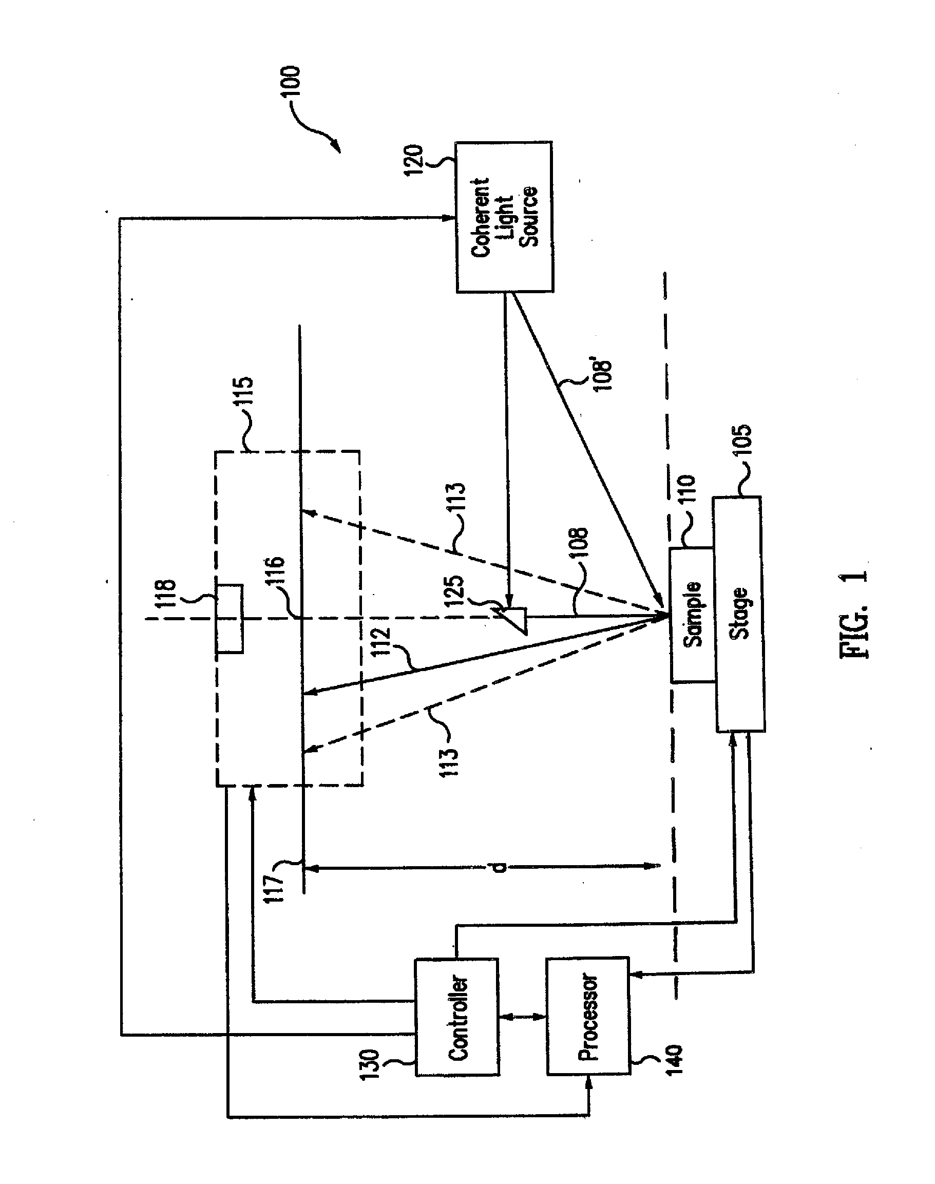
[0037] Systems and techniques provided herein may allow for efficient and accurate sample characterization. Both patterned and unpatterned wafers may be quickly characterized by analyzing diffraction patterns generated when coherent light is diffracted by a sample. Further, both patterned and unpatterned wafers may be quickly characterized by analyzing a reflected pattern projected on and reflected from wafers when the pattern is generated from a light source. Further, the techniques are non-destructive, so that actual product wafers may be characterized (if desired).

[0038]FIG. 1 shows an embodiment of a system 100 configured to characterize a sample 110, such as a patterned or unpatterned semiconductor wafer. Light is generated by a coherent light source 120, and a probe beam 108 is directed to sample 110 using (for example) a prism 125.

[0039] Sample 110 may be mounted on a stage 105 so that relative movement between sample 110 and probe beam 108 may be provided. Stage 105 may be...


PUM


Abstract

Systems and techniques for characterizing samples using optical techniques are described. Light may be incident on a sample in the form of a pre-defined pattern which impinges on a wafer surface, and a reflection of the pattern is detected at a detector. Information indicative of changes in the pattern after reflection may be used to determine one or more sample characteristics and / or one or more pattern characteristics, such as stress, warpage, and curvature. The light may be coherent light of a single wavelength, or may be light of multiple wavelengths, and the pattern may be generated by transmission of the light through a diffraction grating, or hologram. The light source may be incoherent or multi-wavelength, and the pattern may be generated by imaging a pattern disposed on a mask on the sample and re-imaging the pattern at the detector.

Description

CROSS REFERENCE TO RELATED APPLICATIONS [0001] This application is a Continuation-In-Part application of U.S. patent application Ser. No. 11 / 291,246, entitled “Optical Sample Characterization System”, filed on Nov. 30, 2005.BACKGROUND [0002] 1. Field of Invention [0003] This invention generally relates to wafer processing, and in particularly to measuring wafer stress and patterns. [0004] 2. Related Art [0005] Optical techniques may be used to obtain information about materials. For example, optical techniques may be used to characterize substrates such as semiconductor wafers. Characterization can include measuring stress on the wafer and patterns on the wafer to determine flatness, distortion, warpage, etc. [0006] As the device density on wafers increases, it is more important to quickly obtain accurate information about the unpatterned (blanket) and patterned substrates. However, existing techniques may be time-consuming and cumbersome, and may not sample the wafer adequately. Ad...

Claims


Application Information

Patent Timeline
IPC IPC(8): G01B11/16G01B11/24
CPCG01B11/2513G01B11/306G01N21/4788G01N21/94G01N21/9501G01N21/956G01N21/95607G01N2021/95615G01N2201/1053G03F7/70625H01L21/67288
Inventor YOO, WOO SIKKANG, KITAEK
Owner WAFERMASTERS
Why Eureka
Try Eureka