Methods for improving low k FSG film gap-fill characteristics
- Summary
- Abstract
- Description
- Claims
- Application Information
AI Technical Summary
Benefits of technology
Problems solved by technology
Method used
Image
Examples
Embodiment Construction
I. Introduction
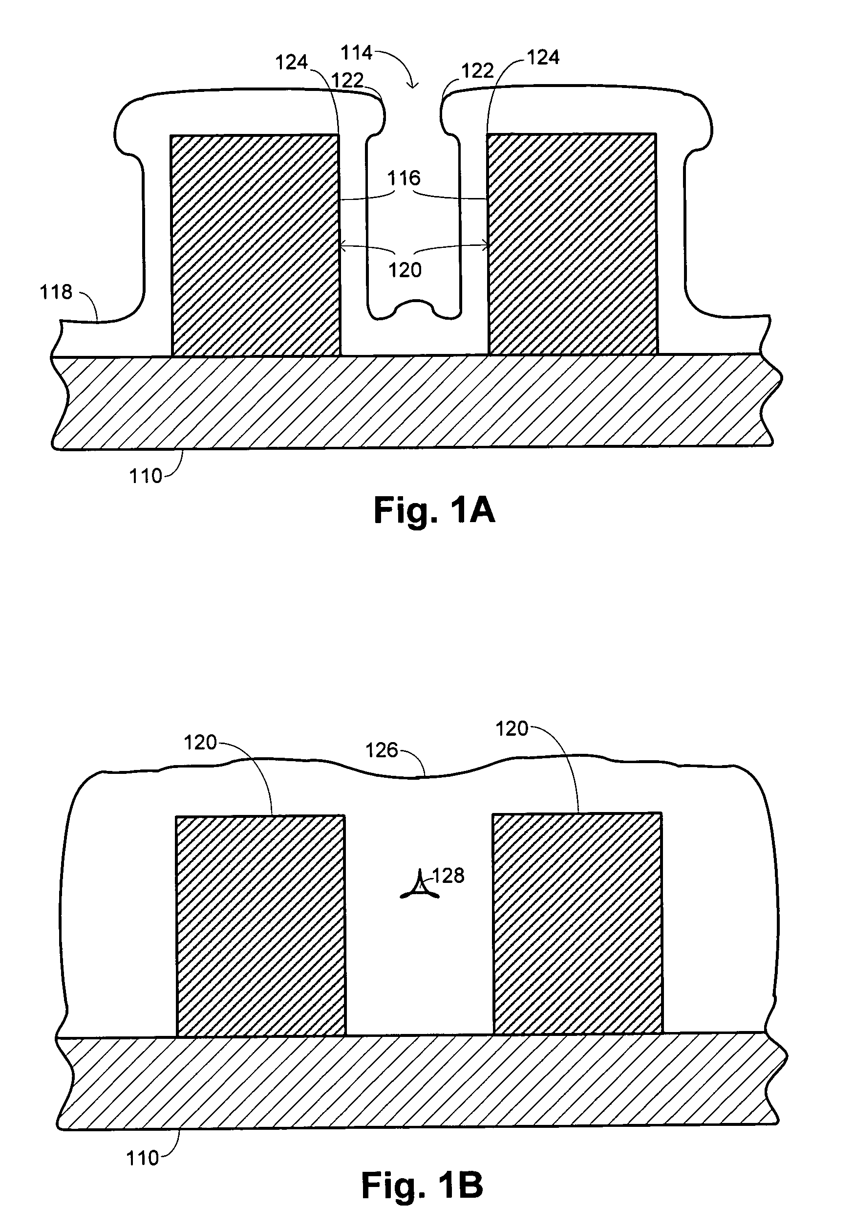
[0018] The gap-fill problem addressed by embodiments of the invention is illustrated schematically with the cross-sectional views shown in FIGS. 1A and 1B. FIG. 1A shows a vertical cross section of a substrate 110, such as may be provided with a semiconductor wafer, having a layer of features 120. Adjacent features define gaps 114 that are to be filled with dielectric material 118, with the sidewalls 116 of the gaps being defined by the surfaces of the fratures 120. As the deposition proceeds, dielectric material 118 accumulates on the surfaces of the features 120, as well as on the substrate 110 and forms overhangs 122 at the corners 124 of the fratures 120. As deposition of the dielectric material 118 continues, the overhangs 122 typically grow faster than the gap 114 in a characteristic bread-loafing fashion. Eventually, the overhangs 122 grow together to form the dielectric layer 126 shown in Fig. 1B, preventing deposition into an interior void 128.
[0019] CVD dep...
PUM
| Property | Measurement | Unit |
|---|---|---|
| Temperature | aaaaa | aaaaa |
| Temperature | aaaaa | aaaaa |
| Length | aaaaa | aaaaa |
Abstract
Description
Claims
Application Information
 - Generate Ideas
- Intellectual Property
- Life Sciences
- Materials
- Tech Scout
- Unparalleled Data Quality
- Higher Quality Content
- 60% Fewer Hallucinations
Browse by: Latest US Patents, China's latest patents, Technical Efficacy Thesaurus, Application Domain, Technology Topic, Popular Technical Reports.
© 2025 PatSnap. All rights reserved.Legal|Privacy policy|Modern Slavery Act Transparency Statement|Sitemap|About US| Contact US: help@patsnap.com


