
Circuit board

a circuit board and circuit board technology, applied in the field of circuit boards, can solve the problems changing the dimension of the antenna, and reducing the efficiency of the antenna, so as to achieve the effect of facilitating modification of the antenna design, and reducing the area occupied by the antenna layou

Inactive Publication Date: 2007-05-03
ARCADYAN
View PDF4 Cites 41 Cited by
  • Summary
  • Abstract
  • Description
  • Claims
  • Application Information

AI Technical Summary

Benefits of technology

[0009] In addition, the invention is to provide a circuit board that can effectively reduce the antenna layout.
[0010] Moreover, the invention is to provide a circuit board that can avoid interference from other electronic elements.
[0012] As mentioned above, the circuit board of the invention has independent antenna substrate and main substrate. With the connection of the first linking portion and the second linking portion, the antenna substrate and the main substrate are assembled in a substantially vertical configuration. Therefore, when the antenna needs to be modified or replaced, the manufacturer only needs to separate the antenna substrate from the main substrate, and then assembles a desired antenna substrate with the main substrate. In this case, the antenna design can be readily modified, and the designs for the antenna substrate and the main substrate become more flexible. Moreover, the antenna layout is not directly disposed on the main substrate. Therefore, the area occupied by the antenna layout is largely reduced, which can efficiently minimize the product volume. In addition, since the antenna substrate and the main substrate are substantially perpendicular to each other, the height of the antenna can be increased to avoid interference with other electronic devices.

Problems solved by technology

Since the antenna and the signal processing circuit are both formed on the above-mentioned circuit board, they are likely to interfere with each other, resulting in antenna characteristic shifts or efficiency lowering.
For example, the dimension of the antenna might be changed, which is very inconvenient.
Moreover, as the antenna is disposed on the circuit board, its characteristics are thus restricted by the material of the circuit board.
In view of the requirement of more compact wireless communication products, the volume of the circuit board is also shrinking.
The space allocated for the antenna and the signal processing circuit is also limited.
Accordingly, elements in the signal processing circuit may have serious interference with the antenna, causing low transmission efficiency of the circuit board.
For example, if the height of a capacitor is far taller than the antenna, the transmitted data may be distorted.

Method used


Image

  • Circuit board
  • Circuit board
  • Circuit board

Examples


Embodiment Construction

[0021] The present invention will be apparent from the following detailed description, which proceeds with reference to the accompanying drawings, wherein the same references relate to the same elements.

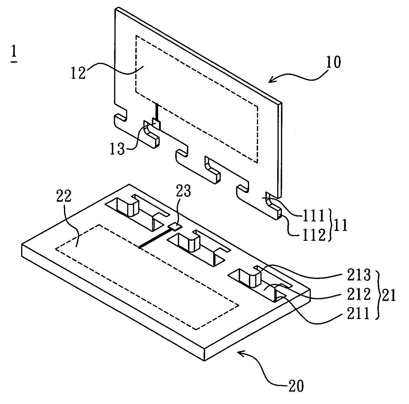
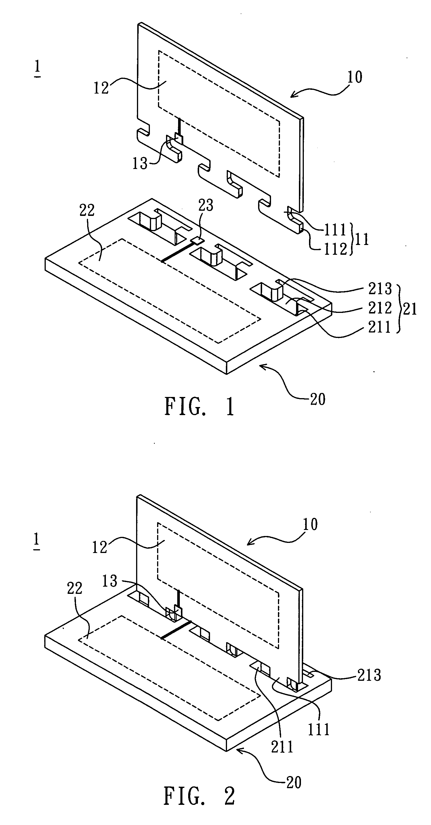
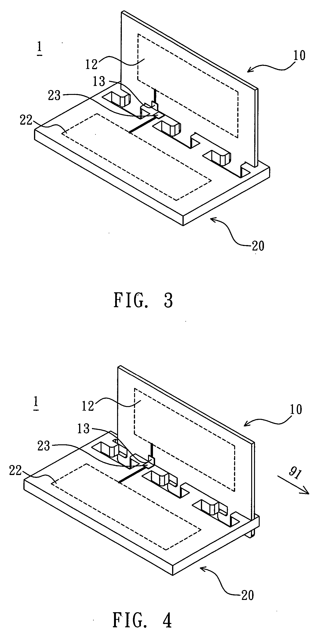
[0022] With reference to FIG. 1, the circuit board 1 according to a preferred embodiment of the invention includes an antenna substrate 10 and a main substrate 20.

[0023] In this embodiment, the antenna substrate 10 has three first linking portions 11, an antenna unit 12 and a first signal terminal 13. It should be noted that even though the number of the first linking portion 11 in this embodiment is three, it is not limited by this example and can be adjusted according to needs. Herein, the antenna substrate 10 can be made of bismaleimide-triazine (BT) resins, FR4 BT epoxy, or ceramics. The antenna unit 12 is embedded in one surface of the antenna substrate 10 to receive and emit wireless signals. The first signal terminal 13 is electrically coupled to the antenna unit 12 for sign...


PUM


Abstract

A circuit board includes an antenna substrate and a main substrate. The antenna substrate has at least one first linking portion. The main substrate has at least one second linking portion. The first linking portion connects with the second portion so that the antenna substrate assembles with the main substrate. Herein, the antenna is substantially perpendicular to the main substrate.

Description

BACKGROUND OF THE INVENTION [0001] 1. Field of Invention [0002] The invention relates to a circuit board and, in particular, to a circuit board with an antenna layout. [0003] 2. Related Art [0004] Due to the progress of the wireless communication techniques, wireless communication devices are widely spread and become the mainstream of modern products such as the wireless network cards, personal digital assistants, mobile phones, Bluetooth earphones, etc. In the wireless communication devices, the antenna is an important element used for receiving and emitting wireless signals. Generally speaking, the conventional wireless communication devices are usually equipped with a circuit board, which is installed with an antenna and a circuit layout for processing signals. The antenna is used to receive and emit wireless signals. The signal processing circuit processes (modulates or demodulates) the wireless signals. [0005] Since the antenna and the signal processing circuit are both formed ...

Claims


Application Information

Patent Timeline
IPC IPC(8): H01Q1/24
CPCH01Q1/243H01Q9/40H05K3/366H05K2201/048H05K2201/09854H05K2201/10598H05K2201/10863H05K2201/2027
Inventor LEE, CHANG-JUNG
Owner ARCADYAN
Learn More