
Resist film removing method

a resist film and removal method technology, applied in the direction of cleaning using liquids, lighting and heating apparatus, instruments, etc., can solve the problems of difficult to remove resist film from the substrate, substrate may be damaged, and it is difficult to remove resist film by wet cleaning of the substra

Inactive Publication Date: 2007-04-12
TOKYO ELECTRON LTD
View PDF2 Cites 9 Cited by
  • Summary
  • Abstract
  • Description
  • Claims
  • Application Information

AI Technical Summary

Benefits of technology

[0010] An object of the present invention is to provide a resist film removing method that allows a resist film having a less-strippable cured layer at the surface to be effectively removed from a substrate without damaging the substrate.
[0025] According to the first aspect of the present invention, a resist film having a cured layer at a surface is covered with a protection film, and then popping is caused in the resist film while it is covered with the protection film. With this arrangement, the cured layer can be widely broken to effectively improve the liquid permeability of the resist film, while droplets of a non-cured part inside the resist film are prevented from being scattered onto the substrate and the substrate is prevented from being damaged. Consequently, it is possible to effectively remove the resist film from the substrate by a predetermined liquid.
[0026] According to the second aspect of the present invention, a resist film having a cured layer at a surface is covered with a thermally shrinkable shrink material, and then the shrink material is shrunk by heating to generate cracks in the cured layer of the resist film. With this arrangement, the cured layer can be widely broken to effectively improve the liquid permeability of the resist film, while droplets of a non-cured part inside the resist film are prevented from being scattered onto the substrate and the substrate is prevented from being damaged. Consequently, it is possible to effectively remove the resist film from the substrate by a predetermined liquid.
[0027] According to the third aspect of the present invention, a resist film having a cured layer at a surface is covered with a softening material capable of softening the cured layer, and then the cured layer is softened in this sate. With this arrangement, the liquid permeability of the resist film can be effectively improved, while droplets of a non-cured part inside the resist film are prevented from being scattered onto the substrate and the substrate is prevented from being damaged. Consequently, it is possible to effectively remove the resist film from the substrate by a predetermined liquid.

Problems solved by technology

In this respect, where the resist film is used for ion implantation of a high concentration, a less-strippable cured layer is formed on the surface of the resist film, so it becomes difficult to peel off the resist film from the substrate.
However, the substrate may be damaged due to the plasma ashing process performed on the resist film.
If the droplets are deposited on the substrate, it is difficult to remove them by wet cleaning of the substrate.
If the heating temperature is set higher for this purpose, the resist film may cause popping, thereby allowing droplets of a non-cured part to be scattered onto the substrate.
Accordingly, this technique is tolerant of crack generation only to the extent that does not entail popping of the resist film, resulting in difficulty in sufficiently removing the resist film.

Method used


Image

  • Resist film removing method
  • Resist film removing method
  • Resist film removing method

Examples


Embodiment Construction

[0037] Embodiments of the present invention will now be described with reference to the accompanying drawings.

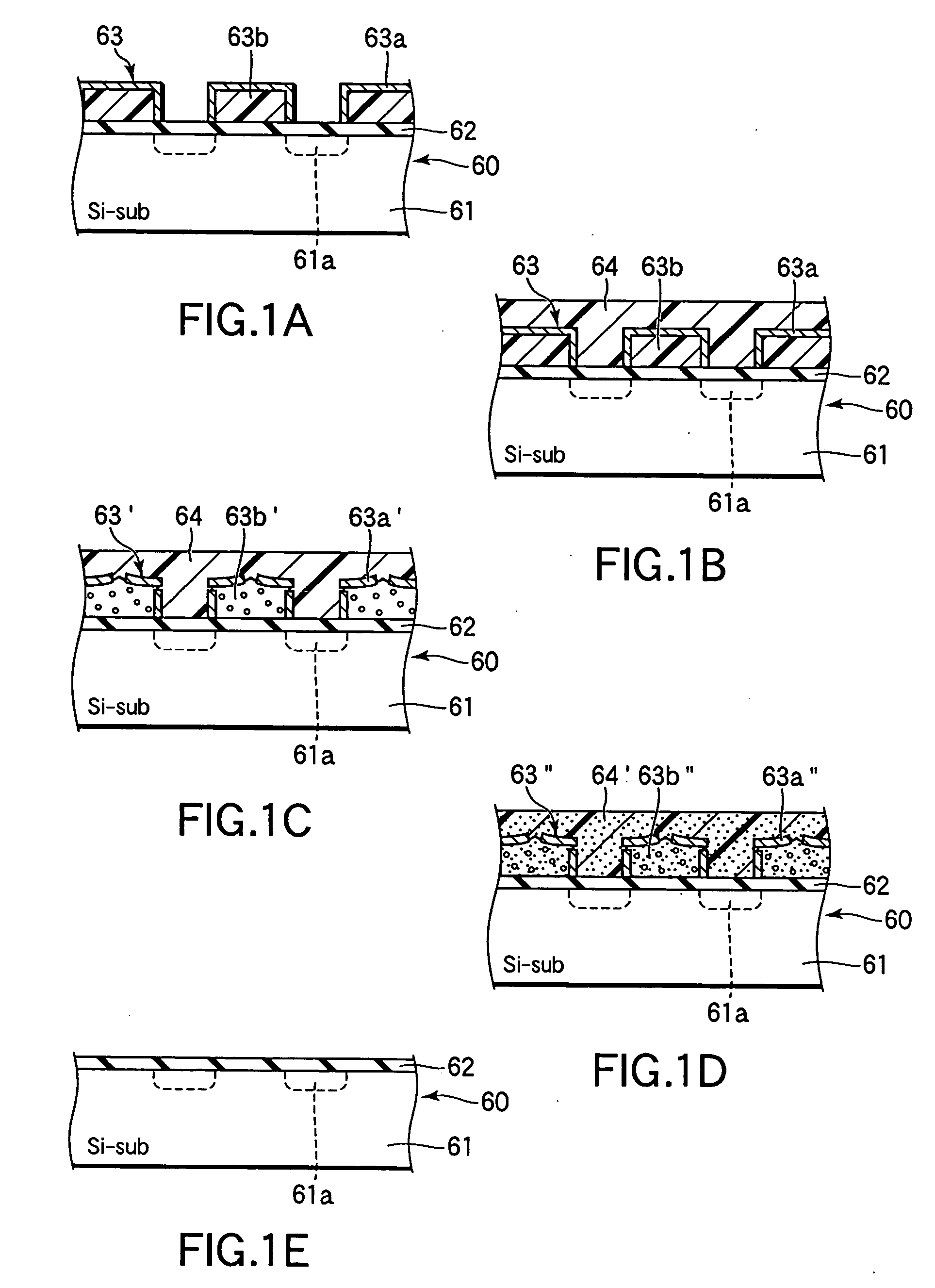
[0038]FIGS. 1A to 1E are views schematically showing steps of a resist film removing method according to an embodiment of the present invention.

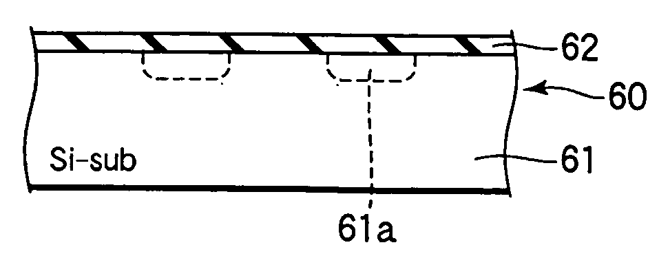
[0039]FIG. 1A shows a state where ion implantation has been performed to form impurity diffusion regions 61a in the main surface of a silicon wafer 61, in the process of manufacturing a semiconductor device. A reference symbol 62 indicates an insulating film formed on the silicon wafer 61, and a reference symbol 63 indicates a resist film formed on the insulating film 62 and used as a mask for the ion implantation. The resist film 63 has been subjected to a light exposure process and a development process, and then to a heating process, before the ion implantation process. A cured layer 63a formed by the ion implantation process of a high concentration is present at the surface of the resist film 63, but a non-cured state (which wi...


PUM


Abstract

A resist film removing method for removing a resist film disposed on a substrate and having a cured layer at a surface includes covering the surface of the resist film with a protection film; causing popping in the resist film covered with the protection film; denaturing the resist film and the protection film after causing popping, to be soluble in water; and performing purified water cleaning to remove from the substrate the resist film and the protection film denatured to be soluble in water.

Description

BACKGROUND OF THE INVENTION [0001] 1. Field of the Invention [0002] The present invention relates to a resist film removing method for removing from a substrate a resist film having a surface cured by a process, such as an ion implantation process or etching process. The present invention also relates to a computer readable storage medium that stores a control program for executing a method of this kind. [0003] 2. Description of the Related Art [0004] In manufacturing semiconductor devices, ion implantation techniques are utilized to implant predetermined ions into a semiconductor wafer made of a silicon substrate, and various films, such as an insulating film, disposed on the surface of a silicon substrate, so as to change their surface property. For example, a p-n junction can be formed in a substrate by implanting ions of, e.g., arsenic (As), phosphorous (P), and / or boron (B) into the substrate. [0005] In general, an ion implantation process is performed after a resist film havin...

Claims


Application Information

Patent Timeline
IPC IPC(8): H01L21/302H01L21/461
CPCG03F7/42G03F7/423G03F7/422G03F7/70491G03F7/70808H01L21/67017H01L21/67028
Inventor ORII, TAKEHIKOSEKIGUCHI, KENJIIINO, TADASHI
Owner TOKYO ELECTRON LTD
Learn More