
Semiconductor device and method for fabricating the same

a semiconductor and semiconductor technology, applied in the direction of semiconductor devices, electrical equipment, transistors, etc., can solve the problems of disadvantageous leakage current flowing along the dislocation loop defect layer, difficult for the conventional method for fabricating a semiconductor, and inability to provide a desired dopant profile of the transistor, etc., to suppress the increase in leakage current flow and increase the concentration of dopants

Inactive Publication Date: 2007-03-22
PANASONIC CORP
View PDF32 Cites 7 Cited by
  • Summary
  • Abstract
  • Description
  • Claims
  • Application Information

AI Technical Summary

Benefits of technology

[0016] With the foregoing problems in mind, an object of the present invention is to ensure an increased dopant concentration of a dopant-diffused channel layer of a semiconductor device while the appearance of short channel effect accompanied with the miniaturization of the device is avoided, and to suppress an increase in leakage current flow resulting from a low threshold voltage and a highly doped channel of the device.
[0019] With the method for fabricating a semiconductor device of the present invention, the amorphous-crystal interface is moved down to the position in the substrate located deeper than that of the dopant implantation layer. Therefore, even if the subsequent thermal treatment is performed to restore the crystallinity of the substrate, no amorphous-crystal interface is formed in the dopant implantation layer. This eliminates the probability of occurrence of a dislocation loop defect layer in the dopant implantation layer during the thermal treatment after the heavy ion implantation, which prevents the phenomenon in which the heavy ions implanted in the channel formation region segregate to the dislocation loop defect layer to become inactivated. Moreover, since no dislocation loop defect layer is formed, leakage current flow resulting from the dislocation loop defect layer can be prevented as well.
[0020] It is known that even a relatively small dose of heavy ions generally amorphizes part of a semiconductor substrate because of their mass effect. In the present invention, the amorphous-crystal interface is expanded deeper than the channel formation region. Therefore, even though the heavy ions are implanted into the channel formation region at a higher dose than the extent that the ions induce amorphization of the region, the heavy ions cause no dislocation loop defect layer immediately below the channel formation region during the thermal treatment after the implantation. This suppresses segregation of the heavy ions immediately below the channel formation region, thereby attaining a heavily-doped and abrupt channel formation region with a retrograde profile.
[0030] Preferably, the inventive method further comprises, between the second and third steps, the step of performing a third thermal treatment at such a temperature that the first dopant ions do not diffuse from the dopant implantation layer and that the crystallinity of the amorphous layer is restored, thereby recovering crystal damages caused by the first dopant ions.
[0031] This method restores the crystallinity of the semiconductor substrate with implantation damages introduced by the heavy ion implantation in the first step while the occurrence of residual defects is prevented.

Problems solved by technology

As a result, the conventional method cannot provide a transistor having a desired dopant profile.
Moreover, if the dislocation loop defect layers are formed in the p-diffused channel layer 203, leakage current disadvantageously flows along the dislocation loop defect layers.
As is apparent from the above, it is difficult for the conventional method for fabricating a semiconductor device to form a heavily-diffused channel layer, which is dispensable for a miniaturized transistor, to have a desired dopant concentration.

Method used


Image

  • Semiconductor device and method for fabricating the same
  • Semiconductor device and method for fabricating the same
  • Semiconductor device and method for fabricating the same

Examples


first embodiment

[0054] A first embodiment of the present invention will be described below with reference to the accompanying drawings.

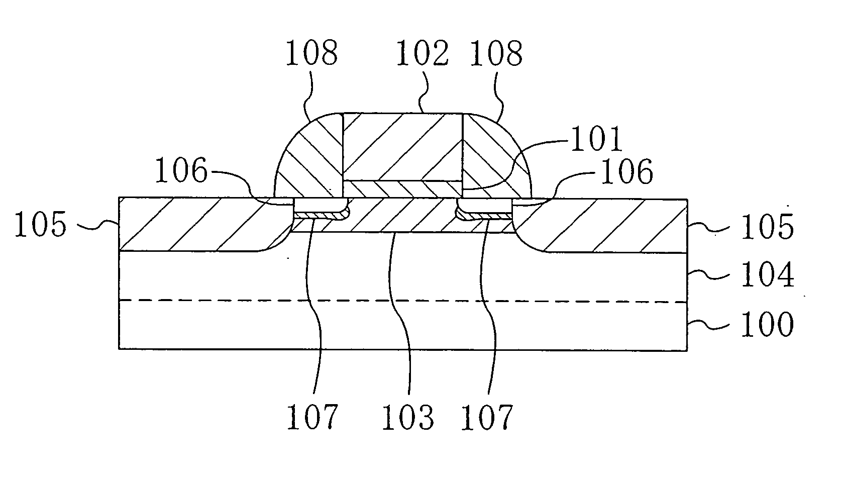
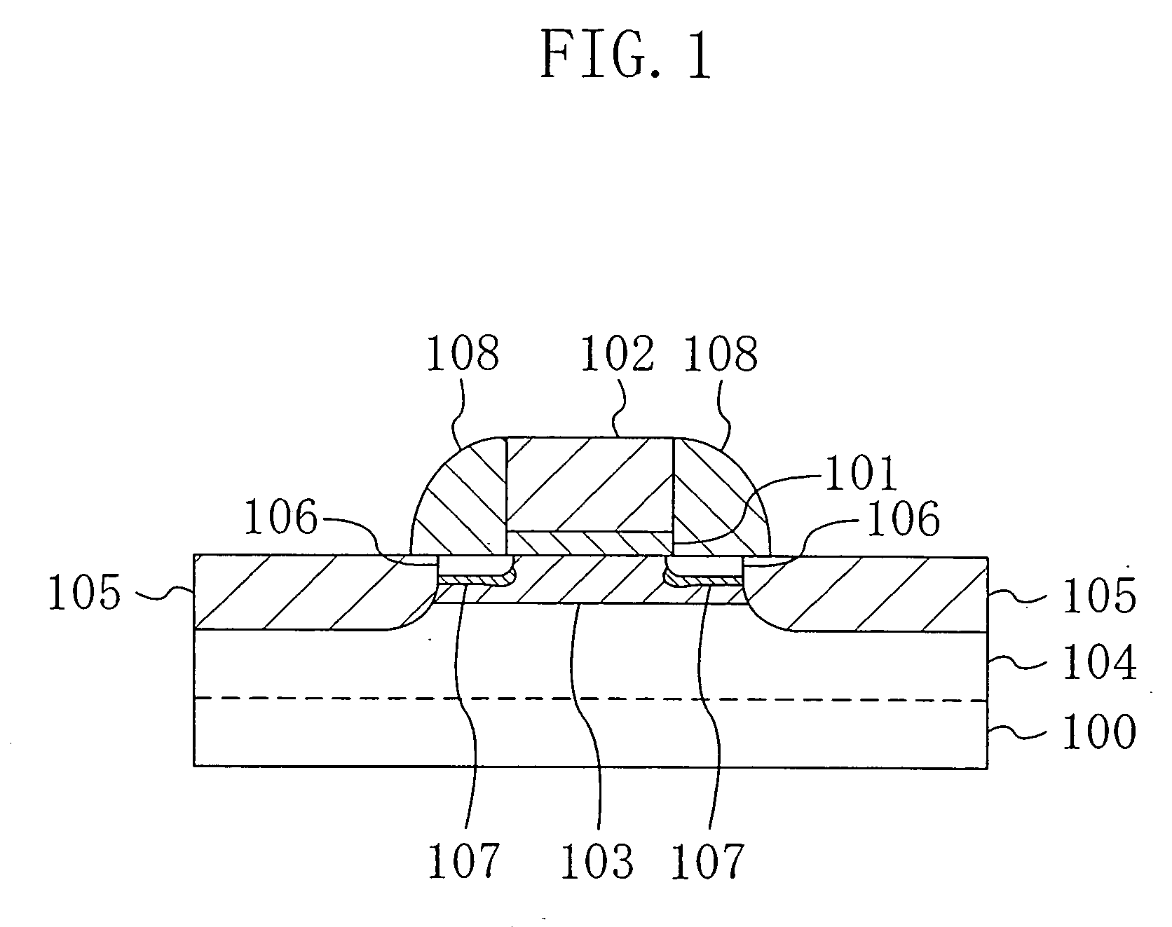
[0055]FIG. 1 shows a cross-sectional construction of a MIS transistor according to the first embodiment of the present invention.

[0056] Referring to FIG. 1, a gate insulating film 101 of silicon oxide is formed on the main surface of a semiconductor substrate 100 of p-type silicon (Si), for example. On the gate insulating film 101, a gate electrode 102 of polysilicon is formed. On the both side surfaces of the gate electrode 102, sidewalls 108 of silicon nitride are formed.

[0057] In a region of the semiconductor substrate 100 located below the gate insulating film 101, a p-diffused channel layer 103 is formed by implanting indium (In) ions which are heavy ions with a relatively large mass number.

[0058] In a region of the semiconductor substrate 100 deeper than the diffused channel layer 103, a germanium (Ge)-containing layer 104 is formed by implanting ions, suc...

second embodiment

[0086] A second embodiment of the present invention will be described below with reference to the accompanying drawings.

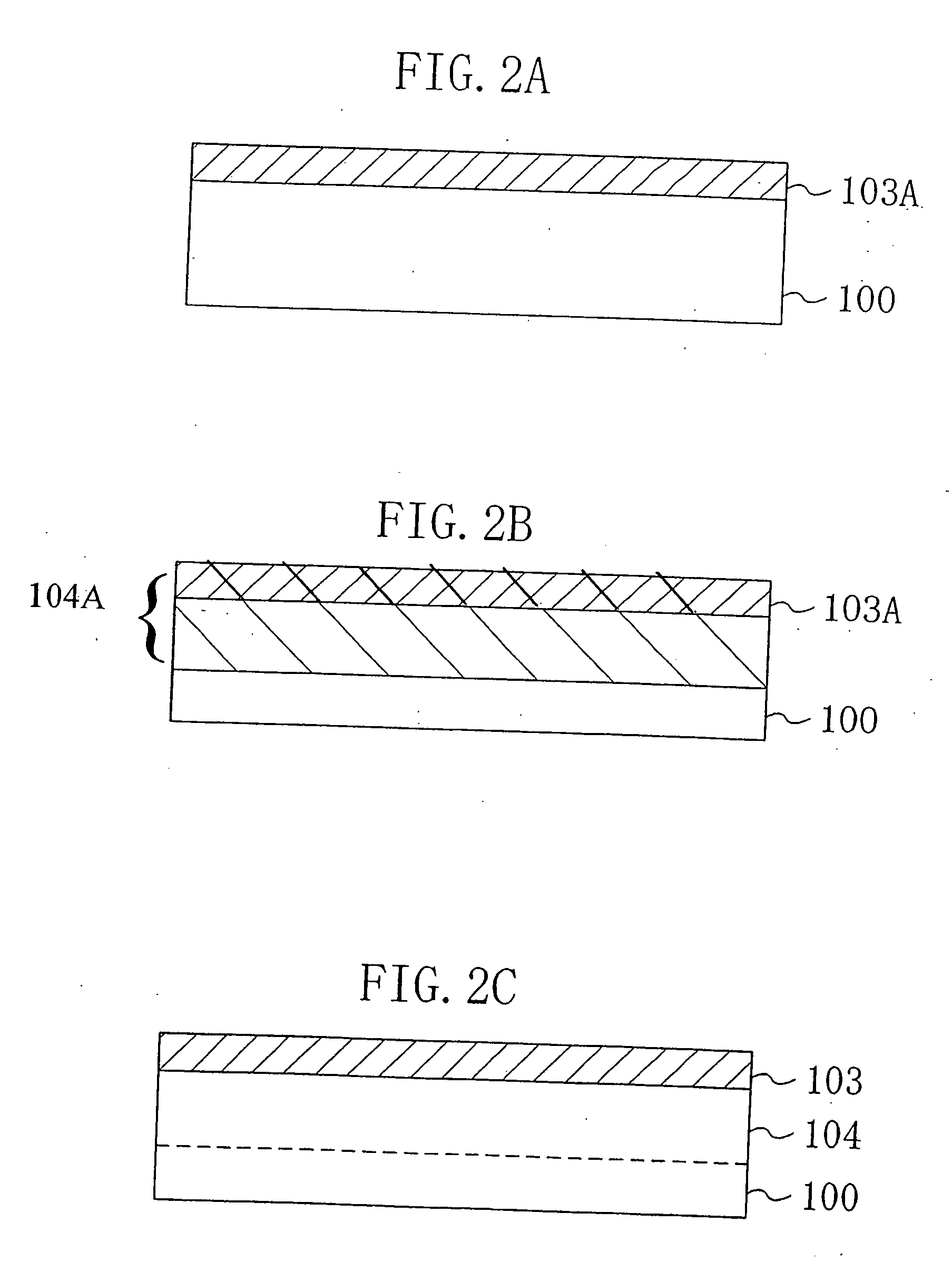
[0087]FIGS. 6A to 6C, 7A to 7C, and 8A to 8C are sectional views showing process steps of a fabricating method of a MIS transistor according to the second embodiment of the present invention step by step.

[0088] First, as shown in FIG. 6A, p-type dopant ions with a relatively large mass number, such as indium (In) ions, are implanted into a channel formation region of a semiconductor substrate 100 made of p-type silicon at an implantation energy of about 70 keV and a dose of about 5×10¹³ / cm2. A p-doped channel layer 103A is thus formed.

[0089] Subsequently, as shown in FIG. 6B, germanium (Ge) ions, for example, belonging to group IV elements are implanted into the upper portion of the semiconductor substrate 100 at an implantation energy of about 250 keV and a dose of about 1×10¹⁶ / cm2, thereby forming an amorphous layer 104A expanding from the substrate surface to...

third embodiment

[0118] A semiconductor device including a strained silicon layer according to a third embodiment of the present invention will be described below with reference to the accompanying drawings.

[0119]FIG. 11A shows a cross-sectional construction of a MIS transistor according to the third embodiment of the present invention. The description of the components shown in FIGS. 11A to 11C that are the same as those shown in FIG. 1 will be omitted by retaining the same reference numerals, and only the difference between the two figures will be described.

[0120] Referring to FIG. 11A, a buffer layer 110 of silicon germanium (Si1-xGex, where 0100. On the buffer layer 110, a strained silicon layer 111 having a thickness of 20 to 50 nm is formed by epitaxially growing silicon.

[0121] As shown in FIG. 11B, when silicon (Si) is epitaxially grown on the buffer layer 110 having a larger lattice constant than silicon, the lattice constant of the resultant strained silicon layer 111 becomes larger (str...


PUM


Abstract

Into a channel formation region of a semiconductor substrate of p-type silicon, indium ions are implanted at an implantation energy of about 70 keV and a dose of about 5×10¹³ / cm2, thereby forming a p-doped channel layer. Next, germanium ions are implanted into the upper portion of the semiconductor substrate at an implantation energy of about 250 keV and a dose of about 1×10¹⁶ / cm2, thereby forming an amorphous layer in a region of the semiconductor substrate deeper than the p-doped channel layer.

Description

RELATED APPLICATIONS [0001] This application is a divisional of U.S. patent application Ser. No. 10 / 676,877 filed Oct. 2, 2003, which is based on Japanese Patent Application No. JP 2002-297513, filed Oct. 10, 2002 the contents of which are hereby incorporated by reference in their entirety.BACKGROUND OF THE INVENTION [0002] The present invention relates to MIS semiconductor devices capable of accomplishing a further miniaturization and operating with high speed and low power consumption, and to methods for fabricating the same. [0003] With increasing packing density of a semiconductor device, MIS transistors in the device are requested to become miniaturized. To accomplish this request, a MIS transistor having a heavily-doped channel structure in which the dopant concentration of a channel region is made high is required (For example, Japanese Unexamined Patent Publication No. 08-250729). [0004] Hereinafter, a conventional method for fabricating a MIS transistor will be described wi...

Claims


Application Information

Patent Timeline
Patent Type & Authority Applications(United States)
IPC IPC(8): H01L29/76H01L29/94H01L21/265H01L21/324H01L21/336H01L29/10
CPCH01L21/26506H01L21/26513H01L21/324H01L29/66628H01L29/1054H01L29/1083H01L29/6659H01L29/105
Inventor NODA, TAIJI
Owner PANASONIC CORP
Learn More