Liquid crystal driving circuit and liquid crystal display device including the same

a driving circuit and liquid crystal technology, applied in the direction of digital storage, pulse automatic control, instruments, etc., can solve the problems of abnormal operation, degradation, and inability to achieve partial driving methods, so as to prolong the life and reduce degradation. the effect of time while high voltage is applied to the gate of each transistor

Active Publication Date: 2007-03-15
INNOLUX CORP
View PDF6 Cites 29 Cited by
  • Summary
  • Abstract
  • Description
  • Claims
  • Application Information

AI Technical Summary

Benefits of technology

[0012] The present invention aims to provide a liquid crystal partial driving circuit in which the degradation of the element is minimized in partial drive even for the GOG circuit configured by amorphous silicon, and the liquid crystal display device applied with the same.
[0016] Therefore, according to the liquid crystal driving circuit and the liquid crystal display device of the present invention, the enable signal is output only for the display target line to be driven by the shift register. The line drive signal is provided by a separate driving means based on the enable signal. Thus, even if partial drive is performed when the driving circuit is formed by amorphous silicon, the time while high voltage is applied to the gate of each transistor is significantly shortened. Therefore, the degradation is prevented, and the extension of longer life is realized.
[0017] Each line address is not directly specified to realize partial drive, but is sequentially specified using a shift register, and thus the number of connecting lines to the outside is greatly reduced, and enhancement of yield and reduction of cost are achieved.

Problems solved by technology

However, such partial driving method is not achieved in a GOG (gate driver on glass) circuit in which a gate made of amorphous silicon transistor is formed on a glass substrate.
This is because degradation of the shift register configured by the amorphous silicon transistor advances when used in such a manner that gate voltage is continuously applied, whereby the threshold value varies and the image quality changes, or leads to abnormality of the operation.
That is, the transistor switch arranged on the line to be partially driven needs to have the transistor turned ON by continuously applying the gate bias while being partially driven in order to perform partial drive, and thus degradation advances in proportion to the time the gate bias is applied, and normal operation cannot be guaranteed over a long period of time.

Method used


Image

  • Liquid crystal driving circuit and liquid crystal display device including the same
  • Liquid crystal driving circuit and liquid crystal display device including the same
  • Liquid crystal driving circuit and liquid crystal display device including the same

Examples


first embodiment

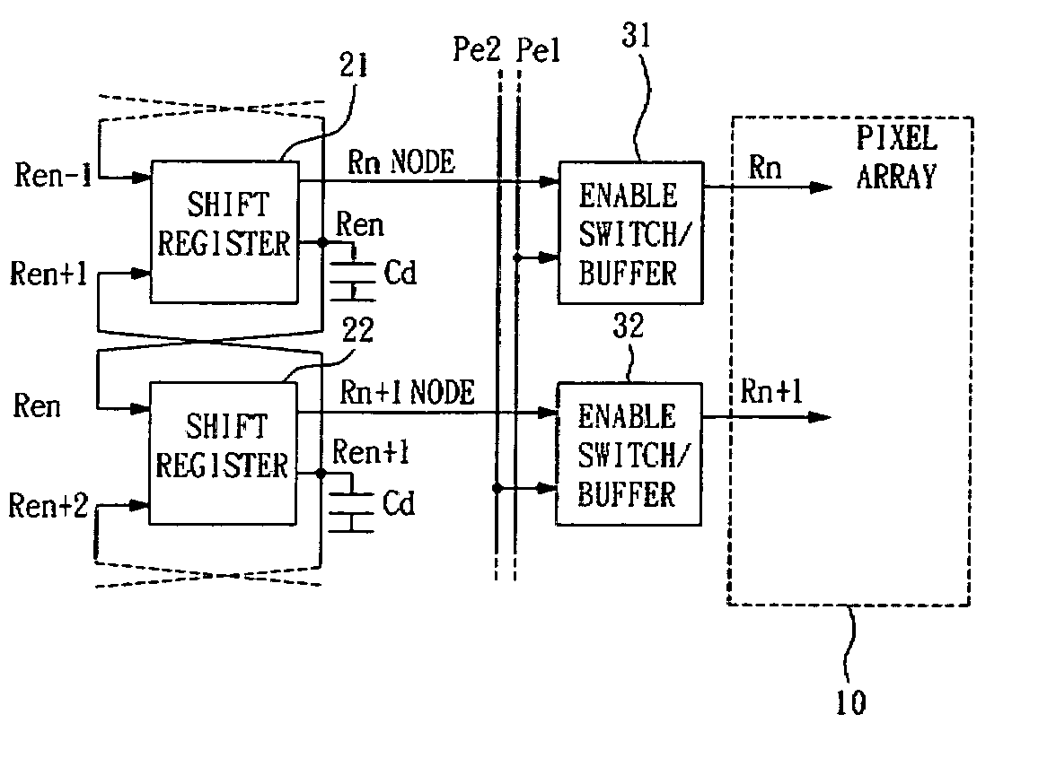
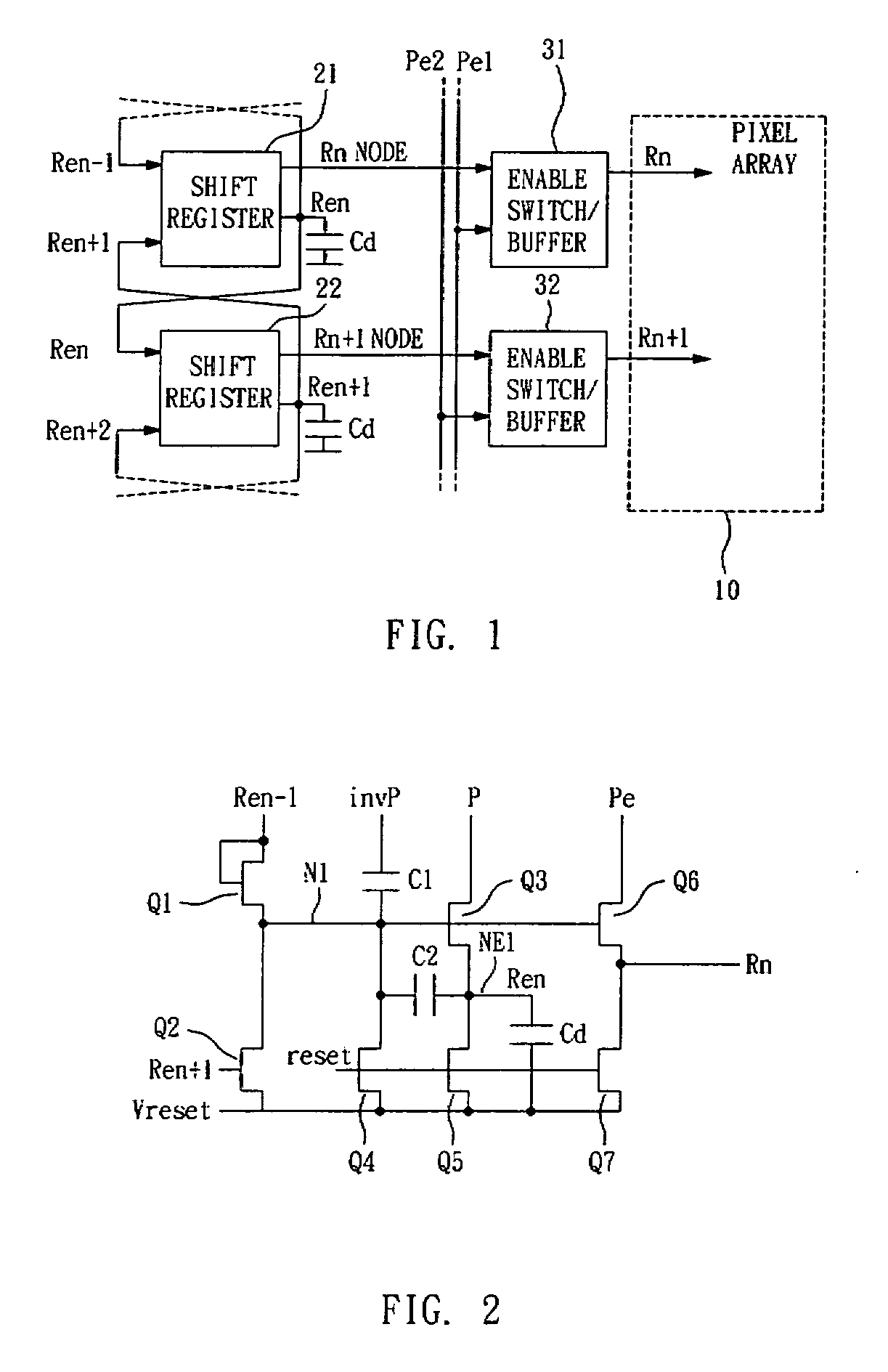
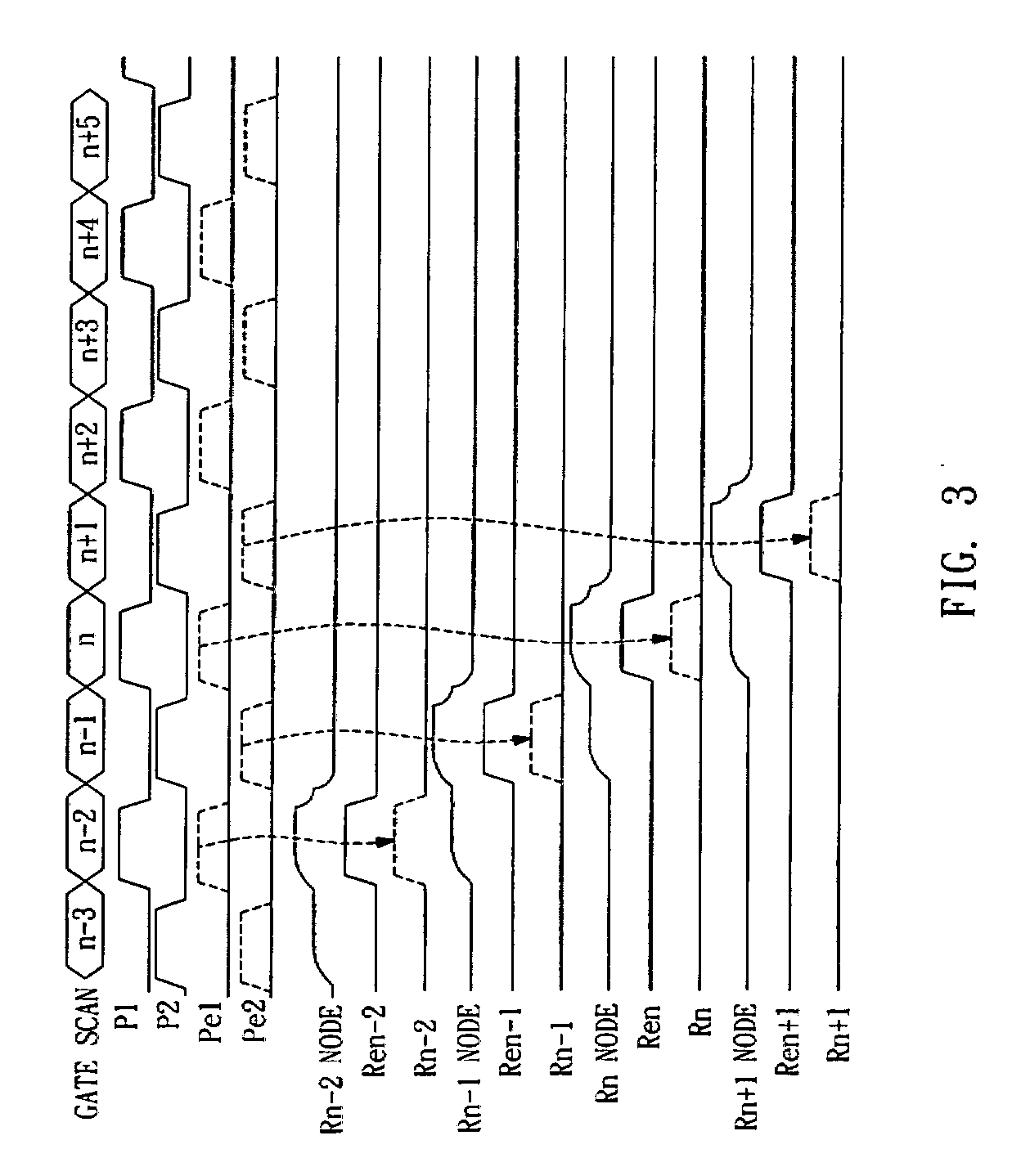
[0029]FIG. 1 is a simplified configuration view showing one part of the configuration according to one embodiment of a liquid crystal driving circuit of the present invention. FIG. 1 illustrates the configuration of sending the drive signal to two row lines (n and n+1) with respect to a pixel array 10. In the pixel array 10, the liquid crystal display elements are arranged in a matrix form.

[0030] With respect to line n, the signal Pe1 on an enable line is output as a signal Rn for the pixel array 10 via an enable switch / buffer 31 by the output of a shift register 21. Similarly, with respect to line n+1, the signal Pe2 on an enable line is output as a signal Rn+1 for the pixel array 10 via an enable switch / buffer 32 by the output of a shift register 22.

[0031] The shift register has the output of the node (Rn node) of the relevant line. In addition, the shift register has an enable output Ren. The enable output Ren is used to charge a dummy capacitor Cd and is input to the shift reg...

second embodiment

[0046] FIGS. 4 to 6 show the configuration and the operation according to a second embodiment of the liquid crystal driving circuit according to the present invention. FIG. 4 is a simplified view showing the configuration, which configuration differs from the configuration of FIG. 1 in that the shift registers are arranged on both sides of the liquid crystal pixel array 10 with one side for moving to the line to be displayed and the other side for providing the selective pulse to the gate line of the pixel array.

[0047]FIG. 4 shows the configuration for the two lines of n and n+1. The shift registers 51, 52 on the right side are a second shift register for advancing through the lines. The registers 41, 42 on the left side are a first shift register for the pixel array 10 to perform the line drive. A switch SW is arranged adjacent to the pixel array 10 for connecting the output line of the second shift register and the output line of the first shift register according to the scan sig...

third embodiment

[0061] A third embodiment of the liquid crystal driving circuit according to the present invention will now be described with reference to FIGS. 7 to 9.

[0062]FIG. 7 is a view showing a schematic configuration of the third embodiment of the liquid crystal driving circuit according to the present invention, showing the nth and the n+1th lines, similar to the other embodiments. The first shift register on the left side indicated by reference characters 61 and 62 is a shift register for advancing to a desired address line. Two second shift registers indicated by reference characters 71, 72 are further provided for outputting the signal for line driving the pixel array 10 by the output of the OR gate. The output of an OR gate is a logical product of an output of an AND gate and the enable signal from the previous line. The output of the AND gate is a logical sum of the output of the first shift register and the Scan signal for validating the scan. This circuit supplies high driving volt...


PUM


Abstract

A liquid crystal drive circuit in which the degradation of the element is minimized in partial drive even for the GOG circuit configured by amorphous silicon, and a liquid crystal display device including the same are provided. The liquid crystal driving circuit includes a first shift register and a driving means. The first shift register advances through the line address of a pixel array to display an image, and outputs an enable signal only to drive the display target line. The driving means outputs a line drive signal corresponding to the enable signal to drive the line enabled by the first shift register.

Description

BACKGROUND OF THE INVENTION [0001] This application claims the benefit of Japan Application Ser. No. 2005-262762, filed Sep. 9, 2005. [0002] 1. Field of Invention [0003] The present invention relates to a liquid crystal driving circuit and a liquid crystal display device including the same, in particular, a liquid crystal partial driving circuit configured by a TFT (Thin film transistor) gate driver made of amorphous silicon and capable of performing partial drive in standby, and a liquid crystal display device including the liquid crystal partial driving circuit. [0004] 2. Related Art [0005] The liquid crystal display device has relatively small power consumption. But recently, further reduction in power consumption is desired particularly in the field of portable telephones and the like as a result of demand for extended operation. For example, further reduction in the power consumption is desired even in the reflection type liquid crystal display device although the reflection ty...

Claims


Application Information

Patent Timeline
IPC IPC(8): G09G3/36
CPCG09G3/3677G09G2300/0417G11C19/184G09G2320/043G09G2310/0286
Inventor YAMASHITA, KEITARO
Owner INNOLUX CORP
Why Eureka
Try Eureka