Microlens substrate, a liquid crystal panel and a projection type display apparatus

a liquid crystal panel and microlens technology, applied in non-linear optics, instruments, optics, etc., can solve the problems of aging deterioration in such liquid crystal panels, general deterioration of photocuring resin materials, and difficulty in obtaining opposed substrates for liquid crystal panels having sufficient durability, etc., to achieve excellent optical characteristics and durability.

Inactive Publication Date: 2007-03-01
SEIKO EPSON CORP
View PDF10 Cites 12 Cited by
  • Summary
  • Abstract
  • Description
  • Claims
  • Application Information

AI Technical Summary

Benefits of technology

[0014] It is one object of the invention to provide a microlens substrate for an opposed substrate which has excellent optical characteristics and durability and can be applied to the manufacture of a liquid crystal panel.

Problems solved by technology

However, it has been difficult to obtain an opposed substrate for a liquid crystal panel having sufficient durability in the case of using such a method.
For this reason, since such a liquid crystal panel provided with a microlens substrate formed of a photocuring resin material (in particular, a liquid crystal panel used in a projection type display apparatus which is irradiated with light of high light intensity) is irradiated with beams (light) when used, aging deterioration tends to be generated in such a liquid crystal panel.
Further, a photocuring resin material generally deteriorates heat resistance compared with an inorganic material.
Thus, in the case where a black matrix, a common electrode and the like are formed (coated) on a microlens substrate formed of a photocuring resin material, in particular, in the case where these elements are formed by means of a vapor deposition method, a constituent material of the microlens substrate may be deteriorated.
Further, a photocuring resin material generally has low hardness (stability of a shape) even after photocured compared with the inorganic material, and deformation of the photocuring resin material due to pressure tends to occur.
Therefore, when such a photocuring resin material is used as a constituent material of a liquid crystal panel, deformation or the like may occur.
In the case where the thickness of such a cover glass is too thick, light take-out efficiency (light transmittance) is deteriorated because light condensed by microlenses is focused in the cover glass.
In the case where the thickness of the cover glass is too thick, a problem that light irradiating TFT elements has harmful influence on the TFT elements tends to occur.
However, since it is very difficult to deal with such a cover glass having a relatively thin thickness, a cover glass having an appropriate thickness is generally formed by coating a glass substrate having a sufficient thickness (for example, about 1 mm) on the surface of the substrate (base substrate) formed of the photocuring resin material and then polishing the glass substrate.
Since such polishing requires considerable labor and time, it has much influence on increase of the manufacturing costs of a liquid crystal panel.
Further, since a large number of shavings are generated in such polishing, washing of the substrate has to be carried out during and after the polishing.
Since such washing requires a large volume of water, it is undesired in view of resource saving and an environmental load.
Moreover, there has been possibility that deterioration of the photocuring resin material occurs due to the washing as described above.
As a result, there has been possibility that quality of the opposed substrate for a liquid crystal panel is deteriorated.
Furthermore, even though the washing as described above is fully carried out, particles may remain on the surface of the obtained microlens substrate (opposed substrate for a liquid crystal panel), and this causes the deterioration of the yield of the microlens substrate.

Method used


Image

  • Microlens substrate, a liquid crystal panel and a projection type display apparatus
  • Microlens substrate, a liquid crystal panel and a projection type display apparatus
  • Microlens substrate, a liquid crystal panel and a projection type display apparatus

Examples


example

Example 1

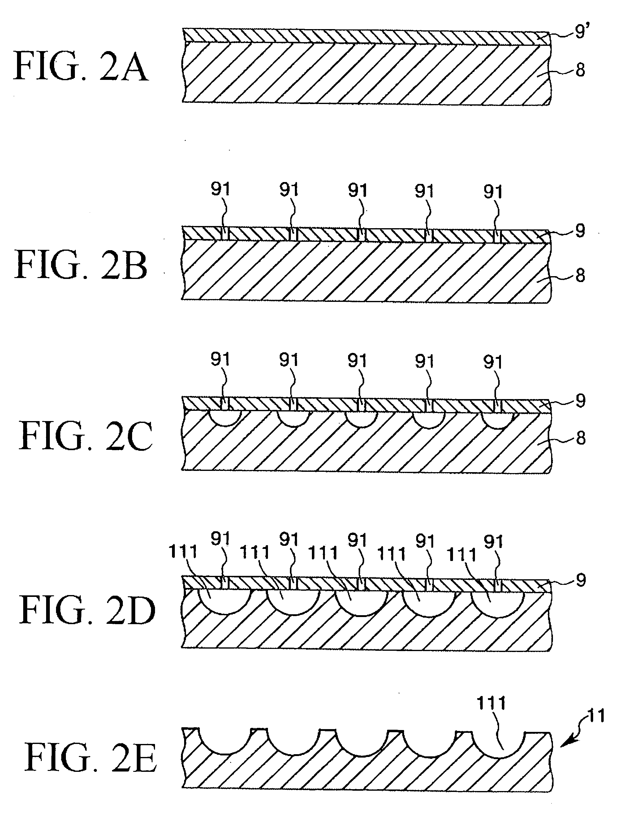
[0190] A substrate with concave portions equipped with a plurality of concave portions was manufactured, and then a microlens substrate was manufactured using the substrate with concave portions in the following manner.

[0191]

[0192] First, a quartz glass substrate (which has an index of refraction of 1.46) having a thickness of 1.2 mm was prepared as a glass substrate.

[0193] The quartz glass substrate was soaked in a cleaning liquid (that is, a mixture of 80% sulfuric acid solution and 20% hydrogen peroxide solution) heated to 85° C. to be washed, thereby cleaning its surface.

[0194] Next, Cr films each having a thickness of 0.03 μm were formed on the quartz glass substrate by means of a spattering method. Namely, a film for forming a mask and a rear face protective film formed of the Cr films were formed on the both major surfaces of the quartz glass substrate.

[0195] Next, a laser machining was carried out with respect to the film for forming a mask, whereby a large num...

examples 2 and 3

[0213] By changing the firming conditions of the initial holes with respect to the film for forming a mask upon manufacturing the substrate with concave portions, the etching conditions and the composition, the composition of an organic-inorganic composite material (epoxy resin-silica composite material) constituting the convex lens substrate, and the property thereof were changed. In this way, microlens substrates (total 100 pieces) were manufactured in a manner similar to that in Example 1 described above except for the above points. In this case, as the spacers in each of Examples 2 and 3, ones formed of the same material as the cured object of the composition were used.

example 4

[0214]

[0215] First, a substrate with concave portions was manufactured in the same manner as that in Example 1.

[0216]

[0217] Next, a composition having fluidity is supplied to the surface of the substrate with concave portions manufactured as described above on which the concave portions are formed. As the composition, one including: an organic-inorganic composite material (acryl based resin-silica composite material) containing polymethylmethacrylate as an organic component and silica as an inorganic component; and methanol as a solvent was used. The viscosity of the composition at room temperature (20° C.) was 1000 mPa·s.

[0218] Further, at this time, in addition to the composition, spacers formed of the organic-inorganic composite material (same as the organic-inorganic composite material as the cured object of the composition) are supplied onto the substrate with concave portions. The spacers each having 30 μm in diameter and a substantially spherical shape was used.

[0219]

[0220...


PUM

PropertyMeasurementUnit
wavelengthaaaaaaaaaa
light transmittanceaaaaaaaaaa
wavelengthaaaaaaaaaa

Abstract

A microlens substrate 1 for an opposed substrate 10 for use in a liquid crystal panel is provided. The microlens substrate 1 includes: a substrate 11 with concave portions formed of a glass material, the substrate 11 with concave portions being provided with a plurality of concave portions 111 on one major surface thereof; and a convex lens substrate 12 provided with a plurality of convex portions 121 each having a shape which corresponds to that of each of the concave portions 111, the plurality of convex portions 121 being provided on one major surface of the convex lens substrate 12 which faces the one major surface of the substrate 11 with concave portions on which the plurality of concave portions 111 are provided. In this case, the convex lens substrate 12 is formed of a constituent material which contains an organic-inorganic composite material as its main material.

Description

CROSS-REFERENCE TO RELATED APPLICATION [0001] This application claims priority to Japanese Patent Application No. 2005-252801 filed on Aug. 31, 2005, which is hereby expressly incorporated by reference herein in its entirety. BACKGROUND OF THE INVENTION [0002] 1. Field of the Invention [0003] The present invention relates to a microlens substrate, a liquid crystal panel and a projection type display apparatus. [0004] 2. Description of the Related Art [0005] There is known a projection type display apparatus that projects an image on a screen. In most of such projection type display apparatuses, a liquid crystal panel (liquid crystal light shutter) is normally used for forming the image. [0006] Such a liquid crystal panel has a configuration in which, for example, an opposed substrate for a liquid crystal panel that is provided with a black matrix, a common electrode and the like is joined to a liquid crystal driving substrate provided with a large number of thin film transistors (TF...

Claims


Application Information

Patent Timeline
Patent Type & Authority Applications(United States)
IPC IPC(8): G02F1/1335
CPCG02F1/133526
Inventor MIYAO, NOBUYUKITANAKA, MITSUTOYO
Owner SEIKO EPSON CORP
Why Eureka
Try Eureka