
Lossless nonlinear analog gain controller in image sensor and manufacturing method thereof

Active Publication Date: 2007-03-01
SAMSUNG ELECTRONICS CO LTD
View PDF12 Cites 40 Cited by
  • Summary
  • Abstract
  • Description
  • Claims
  • Application Information

AI Technical Summary

Benefits of technology

[0010] The ramp signal generator may decrease the slope of the output ramp signal in the low illumination portion and may increase the slope of the output ramp signal in the light illumination portion.

Problems solved by technology

However, when the scene's dynamic range is equal to the sensor's dynamic range, a method of controlling an analog gain by keeping the ramp signal constant may cause data loss, for example, by saturating highlights when increasing the analog gain to brighten shadows.
However, a log sensor suffers from excessive fixed pattern noise (FPN) when transistors in the pixel array are mismatched.
Noise sensitivity and image quality may deteriorate since the CDS method cannot be used, due to the continuous operation of the log sensor.
In addition, the pixel size becomes large due to the number of transistors in the pixel array.

Method used


Image

  • Lossless nonlinear analog gain controller in image sensor and manufacturing method thereof
  • Lossless nonlinear analog gain controller in image sensor and manufacturing method thereof
  • Lossless nonlinear analog gain controller in image sensor and manufacturing method thereof

Examples


Embodiment Construction

[0030] Hereinafter, exemplary embodiments of the present invention will be described in detail with reference to the accompanying drawings. Like reference numerals refer to similar or identical elements throughout the description of the figures.

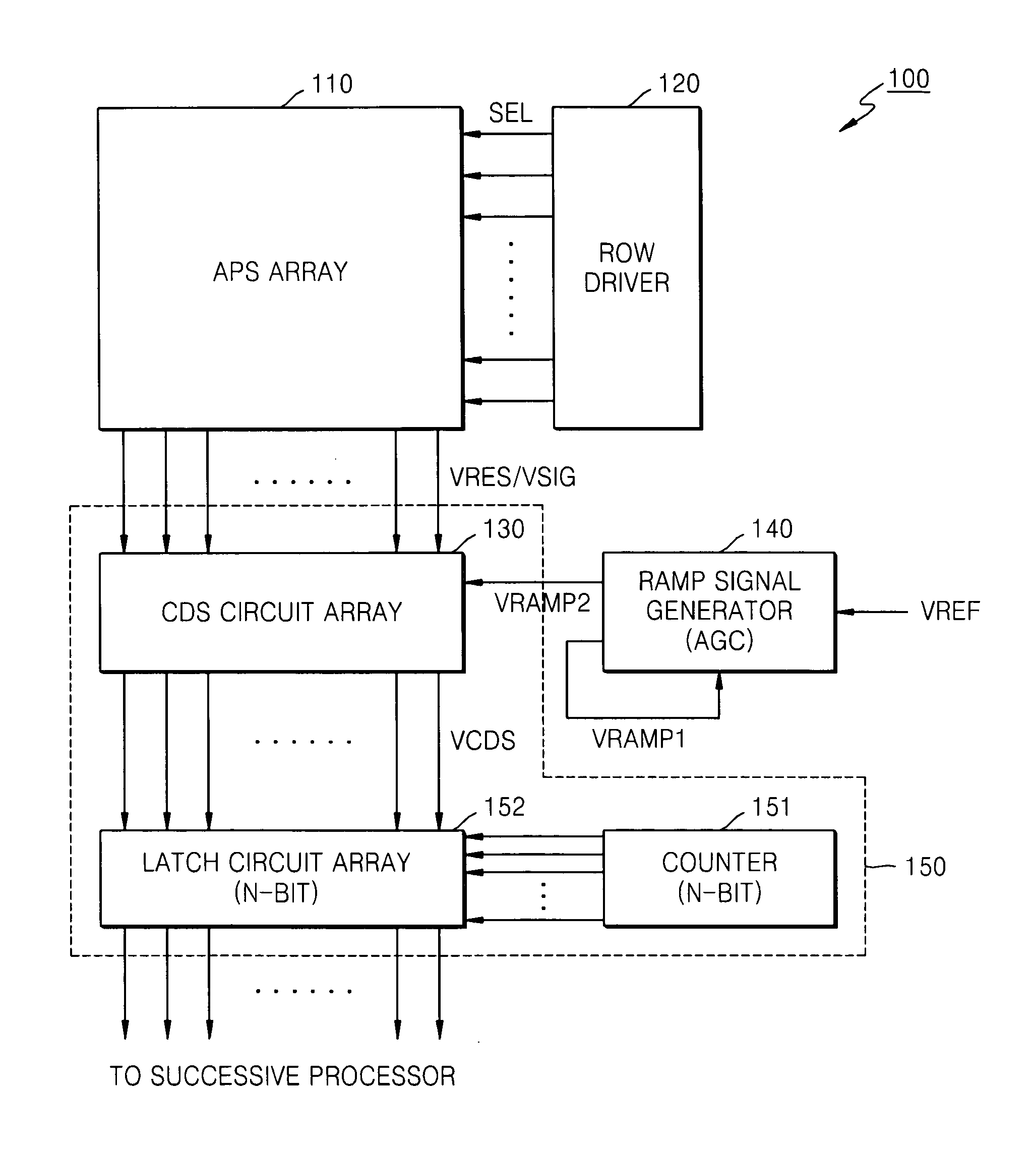
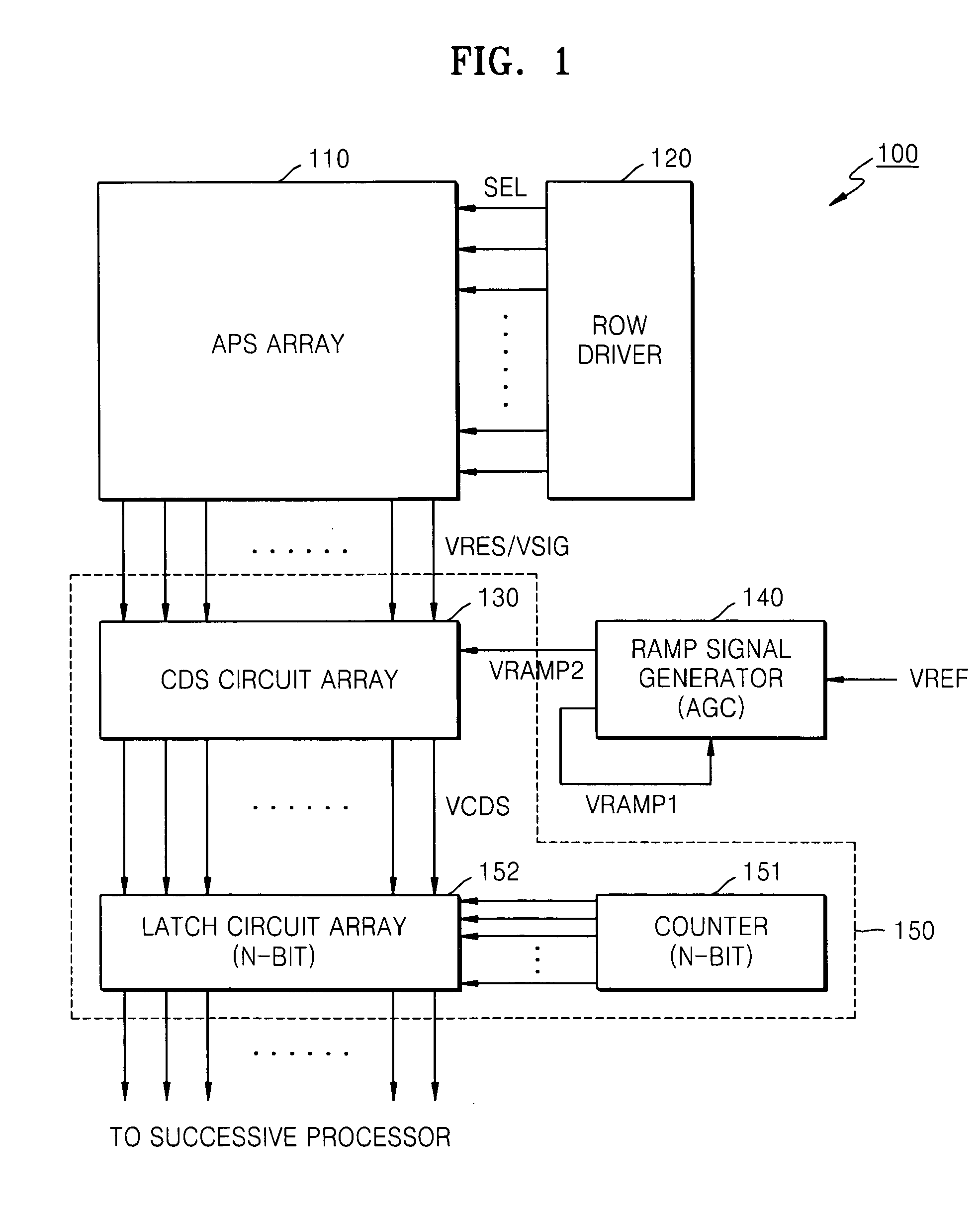
[0031]FIG. 1 shows a CMOS image sensor 100 according to an exemplary embodiment of the present invention. Referring to FIG. 1, the image sensor 100 includes an active pixel sensor (APS) array 110, a row driver 120, a ramp signal generator 140, and a first analog-to-digital converter (ADC) 150. The first ADC 150 includes a correlated double sampling (CDS) circuit array 130.

[0032] The row driver 120 receives a control signal from a row decoder (not shown). A column decoder (not shown) controls an output of pixel data stored in the latch circuit array 152. The image sensor 100 may include a control unit (not shown) which generates overall timing control signals for the image sensor 100, including the first ADC 150 having the CDS circuit array ...


PUM


Abstract

An image sensor comprises an active pixel sensor (APS) array, a first analog-to-digital converter (ADC), and a ramp signal generator. The APS array has includes a plurality of pixels of arranged in a second order two-dimensional matrix, and wherein the APS array generates a reset signal and an image signal for each pixel of selected columns. The first ADC has includes correlated double sampling (CDS) circuits for each column of the APS array, and wherein the first ADC generates a digital code corresponding to the difference between the reset signal and the image signal using an output ramp signal that is applied to the CDS circuits for each column. The ramp generator generates the output ramp signal in which a low illumination portion and a high illumination portion have different slopes.

Description

CROSS-REFERENCE TO RELATED PATENT APPLICATION [0001] This application claims priority to Korean Patent Application No. 10-2005-0078046, filed on Aug. 24, 2005, the disclosure of which is herein incorporated by reference in its entirety. BACKGROUND OF THE INVENTION [0002] 1. Technical Field [0003] The present disclosure relates to an image sensor and, more particularly, to a lossless non-linear analog gain controller in a CMOS image sensor (CIS) type image sensor. [0004] 2. Discussion of Related Art [0005] CMOS image sensors are commonly used in portable cameras, digital still cameras, web cameras and the like to convert an image into a digital signal. The digital image signal that is output from the CMOS image sensor contains red, green, and blue image data. The digital image signal is processed to drive a display device such as a liquid crystal display. [0006] A CMOS image sensor uses a correlated double sampling (CDS) method and uses a ramp signal to generate a digital signal from...

Claims


Application Information

Patent Timeline
IPC IPC(8): H03M1/06H04N5/355H04N5/374H04N5/378H04N9/07
CPCH03M1/123H03M1/58H03M1/56H04N25/57H04N25/75
Inventor HAM, SEOG-HEONHAN, GUNHEE
Owner SAMSUNG ELECTRONICS CO LTD
Learn More