Non-volatile, resistive memory cell based on metal oxide nanoparticles, process for manufacturing the same and memory cell arrangement of the same
- Summary
- Abstract
- Description
- Claims
- Application Information
AI Technical Summary
Benefits of technology
Problems solved by technology
Method used
Image
Examples
Embodiment Construction
[0039]FIG. 1 illustrates a memory element S. Two nanoparticles 10 of, for example, NiO1-x are embedded in an isolating matrix 11 of a dielectric. The nanoparticles 10 contact a bottom contact 9 via contact locations K1 and a top contact 12 via contact locations K2.
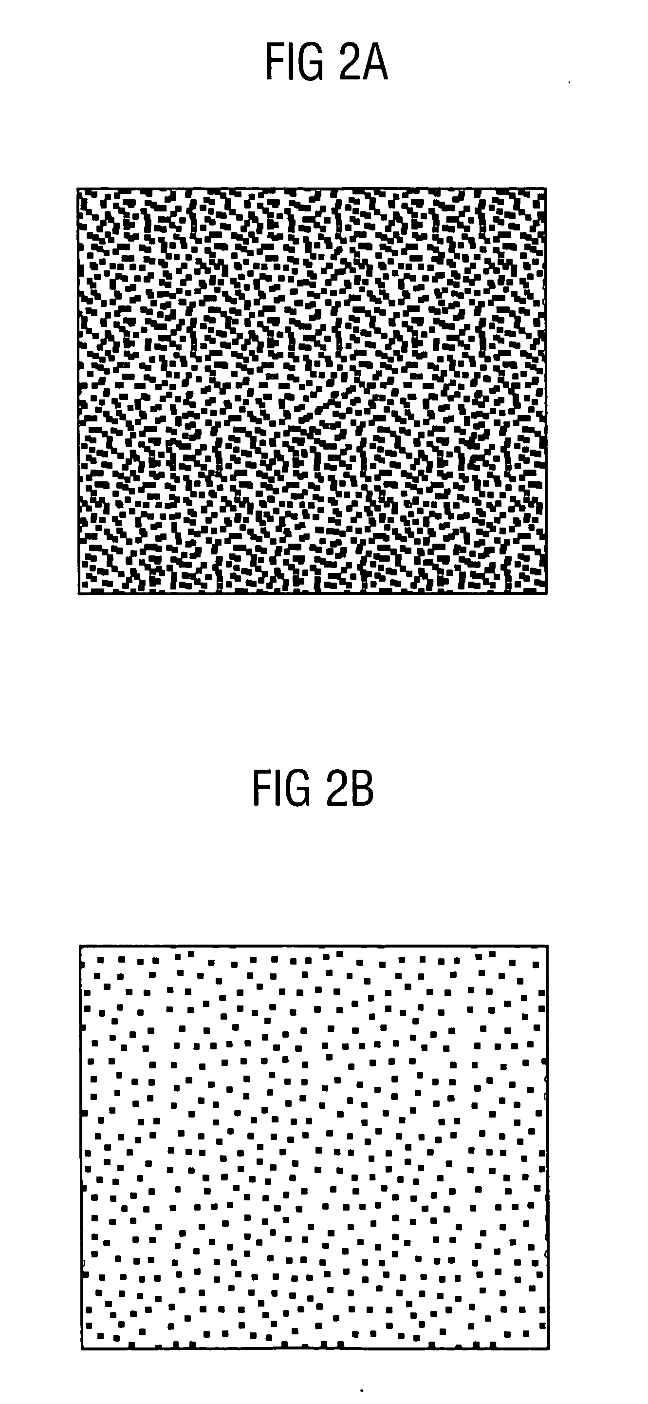
[0040]FIGS. 2a and 2b illustrate a nanoparticle structure with a particle size of 2.9 nm and 7.9 nm, respectively, manufactured in accordance with the embodiment.
[0041]FIG. 3 shows a NiO1-x nanoparticle 10 in an isolating matrix 11 without (left) and with (right) conductive filament. The nanoparticle is contacted by the bottom electrode 9 and the top electrode 12.
[0042]FIGS. 4 and 5 illustrate the configuration of a memory element array. FIG. 4 shows a top view of a memory element array. Word lines 9-1, 9-2 and 9-3 as well as bit lines 12-1, 12-2 and 12-3 are arranged on a substrate 1 made of e.g. silicon. An isolating matrix 11 in which nanoparticles are embedded is arranged between the word lines and the bit lines. Th...
PUM
 Abstract
Description
Claims
Application Information
 - R&D
- Intellectual Property
- Life Sciences
- Materials
- Tech Scout
- Unparalleled Data Quality
- Higher Quality Content
- 60% Fewer Hallucinations
Browse by: Latest US Patents, China's latest patents, Technical Efficacy Thesaurus, Application Domain, Technology Topic, Popular Technical Reports.
© 2025 PatSnap. All rights reserved.Legal|Privacy policy|Modern Slavery Act Transparency Statement|Sitemap|About US| Contact US: help@patsnap.com


