Method and apparatus of pattern inspection and semiconductor inspection system using the same

a technology of semiconductor inspection and pattern inspection, applied in the direction of instruments, nuclear engineering, image enhancement, etc., can solve the problems of pattern deformation, high difficulty in manufacturing such semiconductor devices, and increased frequency of failures in manufacturing processes

Active Publication Date: 2007-02-01
HITACHI HIGH-TECH CORP
View PDF18 Cites 37 Cited by
  • Summary
  • Abstract
  • Description
  • Claims
  • Application Information

AI Technical Summary

Benefits of technology

[0027] As has been explained above, when patterns for a plurality of layers are included in a SEM image photographed, e.g., by a scanning electron microscope (referred to merely as SEM, hereinafter), the pattern inspection apparatus and the semiconductor inspection system of the present invention can accurately measure one of the patterns belonging to one of the layers to be inspected by utilizing the plurality of pieces of design data about the layers corresponding to the patterns.

Problems solved by technology

Since recent semiconductor devices are miniaturized, increased in the number of layers, and made complicated in logic; it is highly difficult to manufacture such semiconductor devices.
As a result, a frequency of failure caused in a manufacturing process tends to increase and it become important to accurately detect its failure position through inspection.
Failures caused by the manufacturing process include pattern deformation caused by improper exposure conditions and continuity failure caused by a positional offset between layers.
This is because the high integration of a semiconductor involves an enormous amount of pattern information.
However, when patterns of a plurality of layers are included in the photographed image, pattern inspection cannot be realized independently for each layer.
In other words, the prior art device does not detect layer information about plural layer patterns included in the photographed image, and performs pattern matching operation with the design-data-based pattern of a single layer corresponding to a superposition of the patterns of the plural layers.
For this reason, when patterns corresponding to a plurality of layers are included in the photographed image, the prior art device has a problem that the device fails to perform the pattern matching operation under the influence of the patterns of the layers other than a target layer to be inspected and thus cannot accurately measure the pattern.
As in the above prior art device, even the disclosed method also has the following problem.
However, this disadvantageously involves an increased processing time, thus reducing an inspection efficiency.

Method used


Image

  • Method and apparatus of pattern inspection and semiconductor inspection system using the same
  • Method and apparatus of pattern inspection and semiconductor inspection system using the same
  • Method and apparatus of pattern inspection and semiconductor inspection system using the same

Examples


embodiment 1

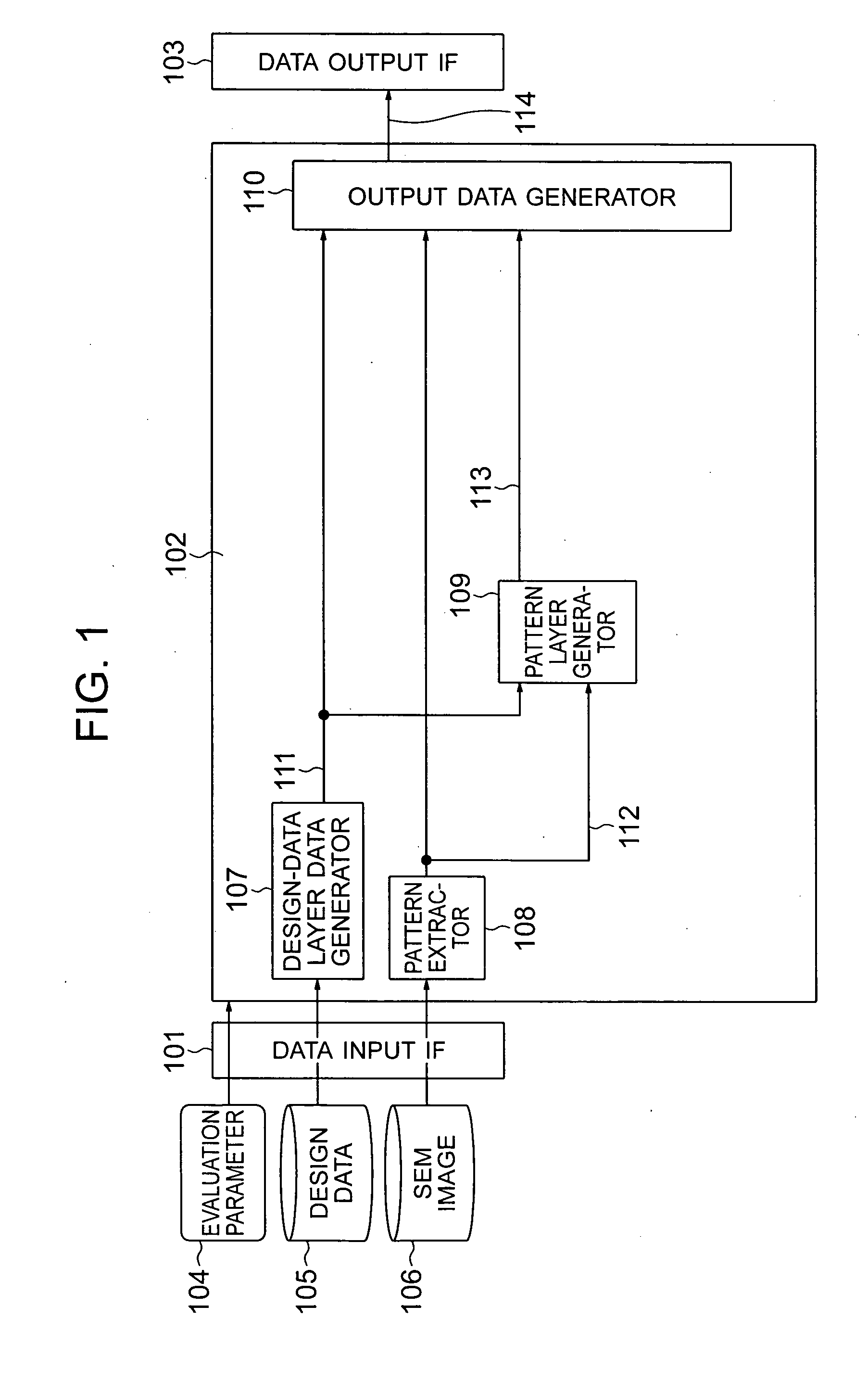
[0057] In the present embodiment, explanation will be made as to the pattern inspection apparatus of the invention for extracting one alone of the layers specified by an operator or by an electronic computer from a SEM image including patterns of a plurality of layers.

[0058]FIG. 1 shows an arrangement of the embodiment 1. The pattern inspection apparatus includes a signal input interface 101, a data calculator 102, and a signal output interface 103. The signal input interface 101 receives a SEM image 106 obtained by photographing a target wafer to be inspected with use of a SEM, design data 105 about a plurality of layers corresponding to pattern images included in the SEM image 106, and various sorts of parameters for evaluation. The data calculator 102 has a design-data layer data layer data of design data generator 107 for generating layer data of design data 111 having a layer structure from the design data 105 of the plural layers, a pattern extractor 108 for extracting patter...

embodiment 2

[0107] Explanation will next be made as to another embodiment.

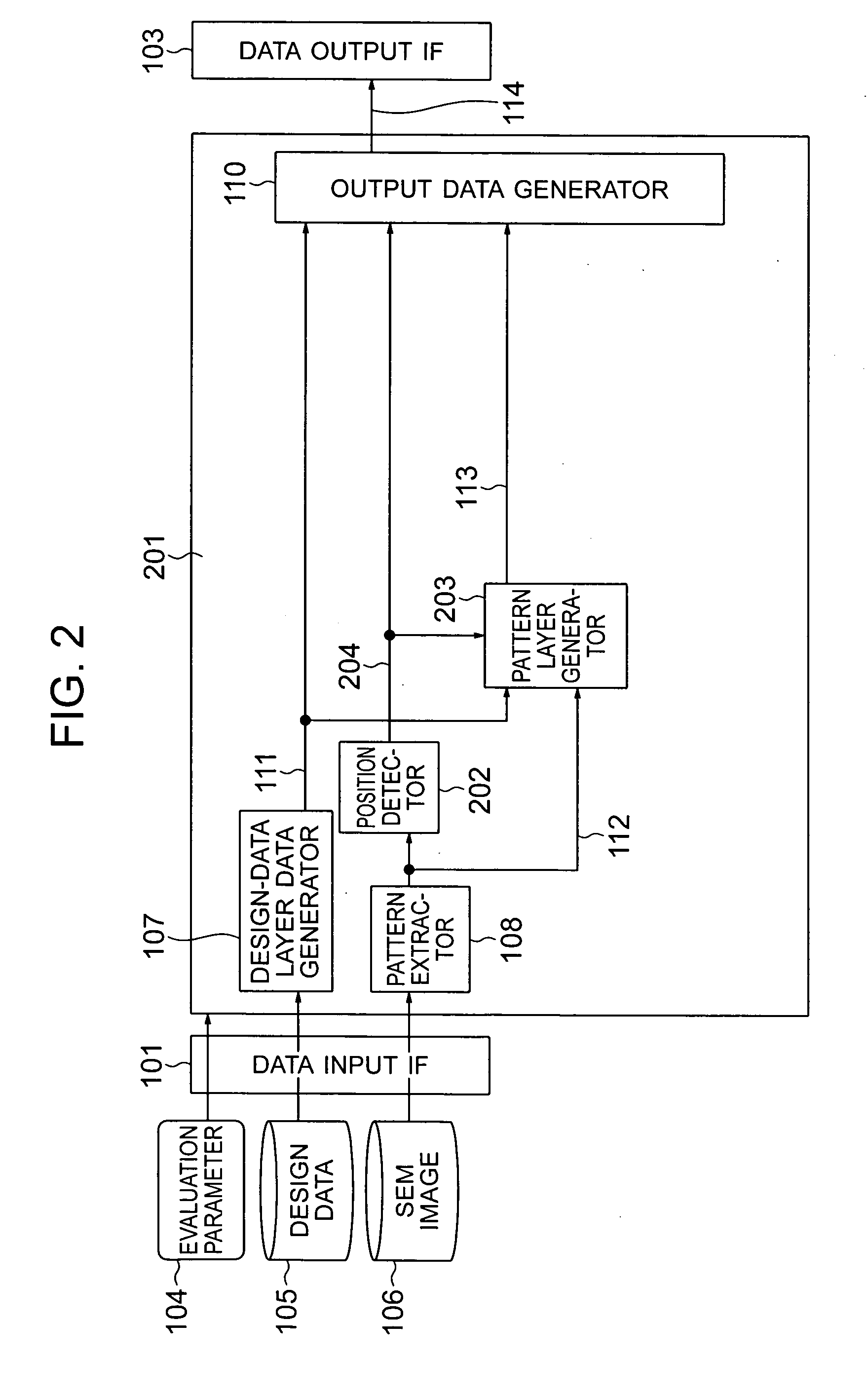
[0108]FIG. 2 shows an arrangement of an embodiment 2.

[0109] In the present embodiment, a position detector 202 is added to the pattern inspection apparatus shown in the embodiment 1. Thus, when a region 601 having design data is different from a region 602 having a pattern of a SEM image as shown in FIG. 6G, the present embodiment performs accurate pattern extraction of a target layer by automatically detecting the position of the pattern corresponding to the design data. In FIG. 6G, a black circle denotes a center position 603 of the SEM image, and a black triangle denotes a center position 604 of the design data.

[0110] The pattern inspection apparatus of the invention will be explained.

[0111] Since the constituent elements of the embodiment 2 other than the position detector 202 and a pattern layer generator 203 are the same as those in the embodiment 1, explanation will be made as to only the position detector 202 ...

embodiment 3

[0118] Explanation will then be made as to a further embodiment of the present invention.

[0119]FIG. 3 shows an arrangement of an embodiment 3.

[0120] In the present embodiment, a layer position detector 301 for performing position detection to identify an inspection position on a pattern by using a pattern of a target layer and design data as well as a pattern measurer 303 for identifying the inspection position on the pattern on the basis of a detected position result and performing pattern measurement inspection, are added to the pattern inspection apparatus shown in the embodiment 1 or 2. Explanation will be made as to a pattern inspection apparatus of the present embodiment which can detect a measurement position using only the pattern of a target layer alone and can measure the pattern.

[0121] The layer position detector 301 is used to detect a position of a target pattern from a SEM image 2300 showing such pattern data as shown in FIG. 23A. More specifically, an inspection po...


PUM


Abstract

A pattern inspection apparatus can be provided, for example, in a scanning electron microscope system. When patterns of a plurality of layers are included in a SEM image, the apparatus separates the patterns according to each layer by using design data of the plurality of layers corresponding to the patterns. Consequently, the apparatus can realize inspection with use of only the pattern of a target layer to be inspected, pattern inspection differently for different layers, or detection of a positional offset between the layers.

Description

BACKGROUND OF THE INVENTION [0001] The present invention relates to a method and apparatus of pattern inspection and a semiconductor inspection system, which inspect a pattern formed on a wafer with use of a photographed image of a semiconductor device and design data on the semiconductor device. [0002] Since recent semiconductor devices are miniaturized, increased in the number of layers, and made complicated in logic; it is highly difficult to manufacture such semiconductor devices. As a result, a frequency of failure caused in a manufacturing process tends to increase and it become important to accurately detect its failure position through inspection. Failures caused by the manufacturing process include pattern deformation caused by improper exposure conditions and continuity failure caused by a positional offset between layers. The locations of such failures are detected by collating design data, such as CAD data (Computer Aided Design data) about a semiconductor device with a ...

Claims


Application Information

Patent Timeline
Patent Type & Authority Applications(United States)
IPC IPC(8): G21K7/00
CPCG06T7/0006H01J2237/2817H01J2237/221G06T2207/30148
Inventor TOYODA, YASUTAKASUGIYAMA, AKIYUKIMATSUOKA, RYOICHISUTANI, TAKUMICHINAYA, HIDEMITSU
Owner HITACHI HIGH-TECH CORP
Why Eureka
Try Eureka