
Methods of making thin film transistors comprising zinc-oxide-based semiconductor materials and transistors made thereby

a technology of zinc oxide-based semiconductor materials and thin film transistors, which is applied in the direction of semiconductor devices, electrical devices, nanotechnology, etc., can solve the problems of wasting materials, amorphous silicon, and requiring relatively difficult or complicated processes,

Active Publication Date: 2006-12-21
EASTMAN KODAK CO
View PDF4 Cites 3840 Cited by
  • Summary
  • Abstract
  • Description
  • Claims
  • Application Information

AI Technical Summary

Benefits of technology

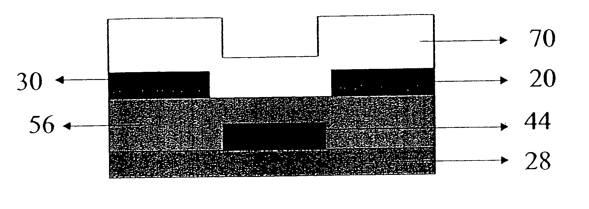
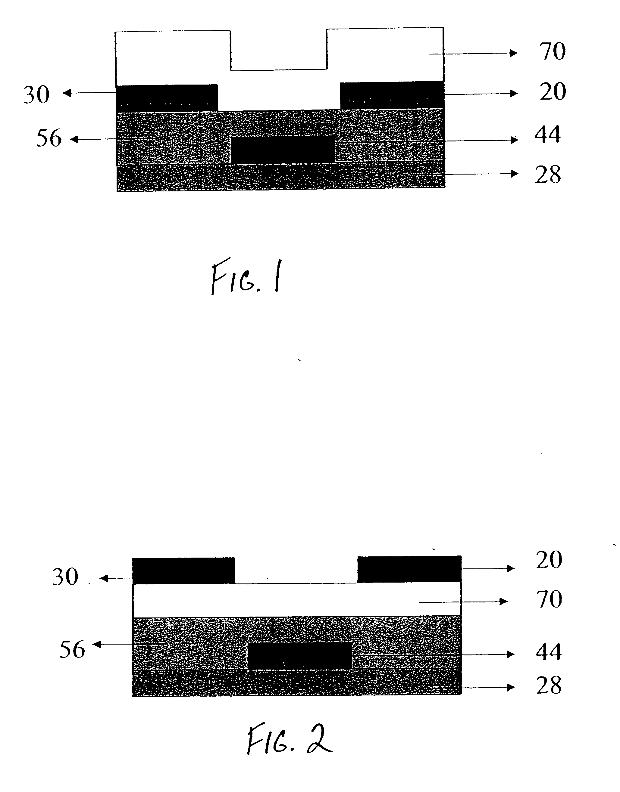
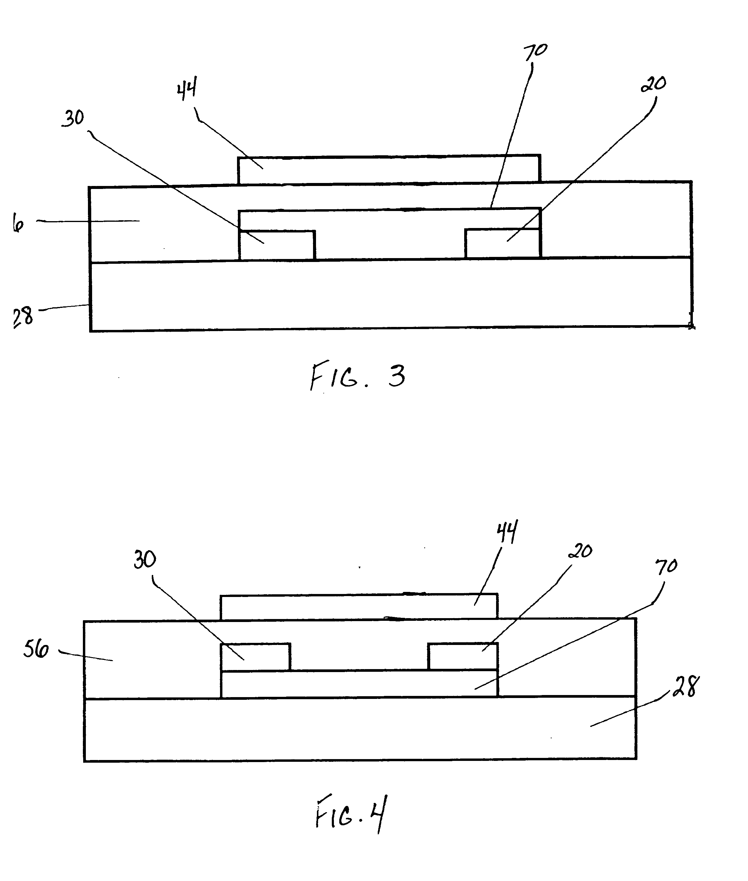
[0031] A TFT structure includes, in addition to the zinc-oxide-based semiconductor, conducting electrodes, commonly referred to as a source and a drain, for injecting a current into the zinc-oxide-based semiconductor. One embodiment of the present invention is directed to the use of such n-channel semiconductor films in thin film transistors each comprising spaced apart first and second contact means connected to an n-channel semiconductor film. A third contact means can be spaced from said semiconductor film by an insulator, and adapted for controlling, by means of a voltage applied to the third contact means, a current between the first and second contact means through said film. The first, second, and third contact means can correspond to a drain, source, and gate electrode in a field effect transistor.

Problems solved by technology

The deposition of amorphous silicon, during the manufacture of transistors, requires relatively difficult or complicated processes such as plasma enhanced chemical vapor deposition and high temperatures (about 360° C.) to achieve the electrical characteristics sufficient for display applications.
These patterning steps are time consuming and waste materials.
Such plastics, however, limit device processing to below 200° C.
However, most organic semiconductors generally have inferior or problematic electronic properties compared to amorphous silicon for use in transistor devices.
For example, organic materials may tend to degrade in normal atmospheric conditions.
The portion of the display glass occupied by the addressing electronics is not available for transmission of light through the display.

Method used


Image

  • Methods of making thin film transistors comprising zinc-oxide-based semiconductor materials and transistors made thereby
  • Methods of making thin film transistors comprising zinc-oxide-based semiconductor materials and transistors made thereby
  • Methods of making thin film transistors comprising zinc-oxide-based semiconductor materials and transistors made thereby

Examples


example 1

[0126] A coating solution was prepared by diluting the above seed formulation, SLF-1, to 1.3% in ethanol. The above solution was applied to the substrate by spin coating at a rate of 2000 rpm. After the spin coating, the samples were annealed for 10 minutes at 200C in dry air. Following the anneal, a precursor layer consisting of zinc acetate dissolved in methanol with concentrations in Samples 1-1 and 1-2 as listed below was spun on to the substrate at 2000 rpm. The methanol solutions can also contain trace levels of water This layer was then annealed at 200° C. for 10 minutes in dry air. After this process, aluminum contacts were applied by evaporation.

[0127] Following contact evaporation, a passivation layer was applied by spin coating. A 2.5% solution of polystyrene in toluene was applied at a rate of 2500 rpm. Following the spin coating, samples were annealed at 60° C. for 5 minutes in air to remove residual solvent. Devices were then tested for transistor activity as describe...

example 2

[0129] Another coating solution was prepared by diluting the above-described seed formulation, SLF-1, to 1.3% in ethanol. The above solution was applied to the substrate by spin coating at a rate of 2000 rpm. After the spin coating, the samples were annealed for 10 minutes at 200° C. in dry air.

[0130] A first sample (2-1) did not receive any precursor overcoat and subsequent anneal. A second sample, 2-2, had the following treatment. A precursor layer consisting of zinc acetate dissolved in methanol at a concentration of 0.175M was spun on to the substrate at 2000 rpm. This layer was then annealed at 200C for 10 minutes in dry air. After this process, Aluminum contacts were applied to both samples by evaporation.

[0131] Following contact evaporation, a passivation layer was applied by spin coating. A 2.5% solution of polystyrene in toluene was applied at a rate of 2500 rpm. Following the spin coating, samples were annealed at 60C for 5 minutes in air to remove residual solvent. Devi...

example 3

[0133] This example shows that the zinc oxide film can be applied by sequentially inkjet printing the ZnO seed nanoparticles and the precursor. Inkjet printing experiments were performed using a system consisting of a sample platen supported by a set of X-Y translation stages, piezoelectric demand-mode printheads supported by a z translation stage, and software to control these components. The printheads of this inkjet system are suited to dispense droplets in the 20-60 picoliter range. Approximately 2 cc of the fluid to be printed is placed in a sample cartridge that is then screwed to the printing fixture. The printhead is primed with ink using pressurized nitrogen. A TENCOR profilometer was used to measure the printed film thicknesses of a series of calibration samples. The drop volume was calculated as 38 picoliters by using best-fit linear regression in a simple model relating number of drops fired, ink concentration, and printed film thickness.

[0134] The inkjet printed ZnO na...


PUM


Abstract

A thin film transistor comprises a zinc-oxide-containing semiconductor material. Such transistors can further comprise spaced apart first and second contact means or electrodes in contact with said material. Further disclosed is a process for fabricating a thin film transistor device, wherein the substrate temperature is no more than 300° C. during fabrication.

Description

FIELD OF THE INVENTION [0001] The present invention relates to the use of zinc-oxide-based semiconductor materials in semiconductor films for thin film transistors. Such thin film transistors can be used in electronic devices, particularly in displays in which solution processable semiconductor materials, and low temperature processes of making the same, are advantageous. BACKGROUND OF THE INVENTION [0002] Thin film transistors (TFTs) are widely used as switching elements in electronics, for example, in active-matrix liquid-crystal displays, smart cards, and a variety of other electronic devices and components thereof. The thin film transistor (TFT) is an example of a field effect transistor (FET). The best-known example of an FET is the MOSFET (Metal-Oxide-Semiconductor-FET), today's conventional switching element for high-speed applications. For applications in which a transistor needs to be applied to a substrate, a thin film transistor is typically used. A critical step in fabri...

Claims


Application Information

Patent Timeline
Patent Type & Authority Applications(United States)
IPC IPC(8): H01L29/22H01L21/00H01L21/84H01L29/786
CPCB82Y10/00H01L21/02472H01L21/02513H01L29/7869H01L21/02579H01L21/02628H01L21/02554
Inventor LEVY, DAVID H.SCUDERI, ANDREA C.IRVING, LYN M.
Owner EASTMAN KODAK CO
Learn More