Method for manufacturing photovoltaic module
- Summary
- Abstract
- Description
- Claims
- Application Information
AI Technical Summary
Benefits of technology
Problems solved by technology
Method used
Image
Examples
Embodiment Construction
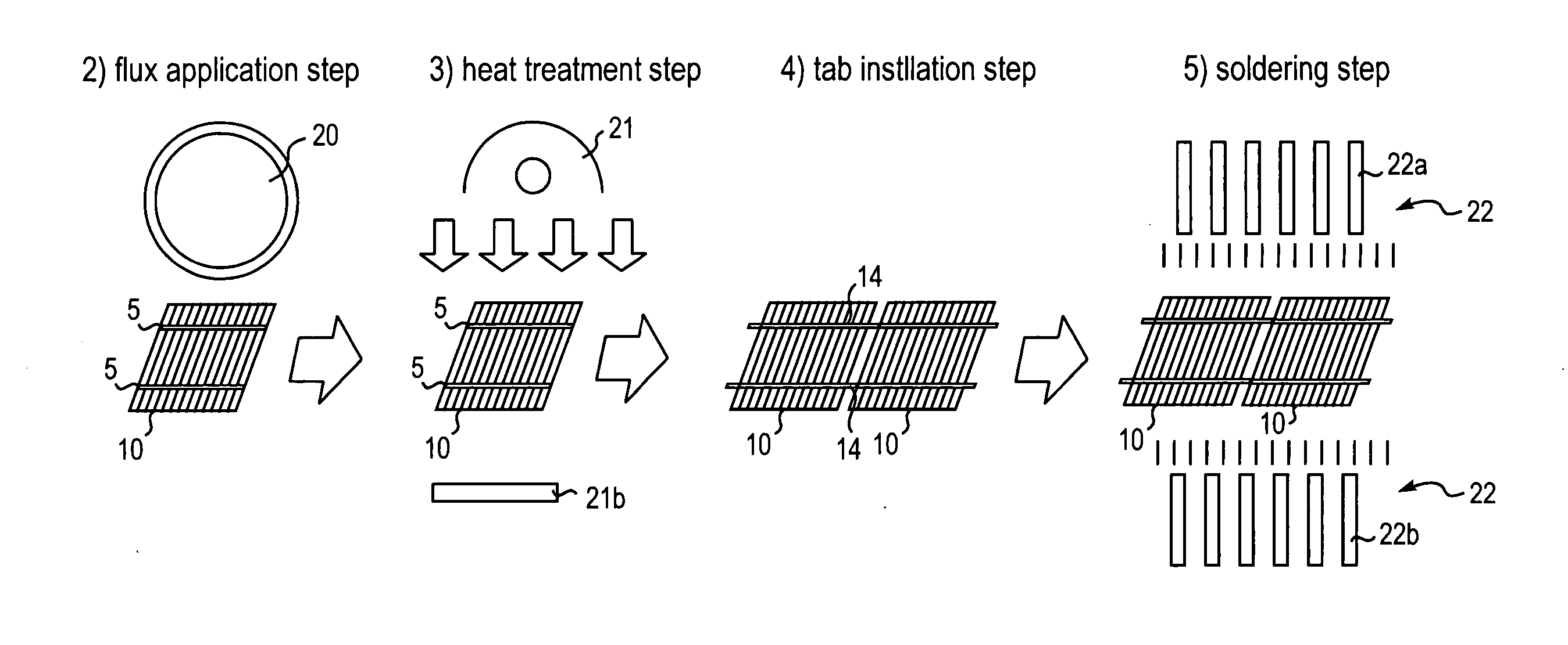
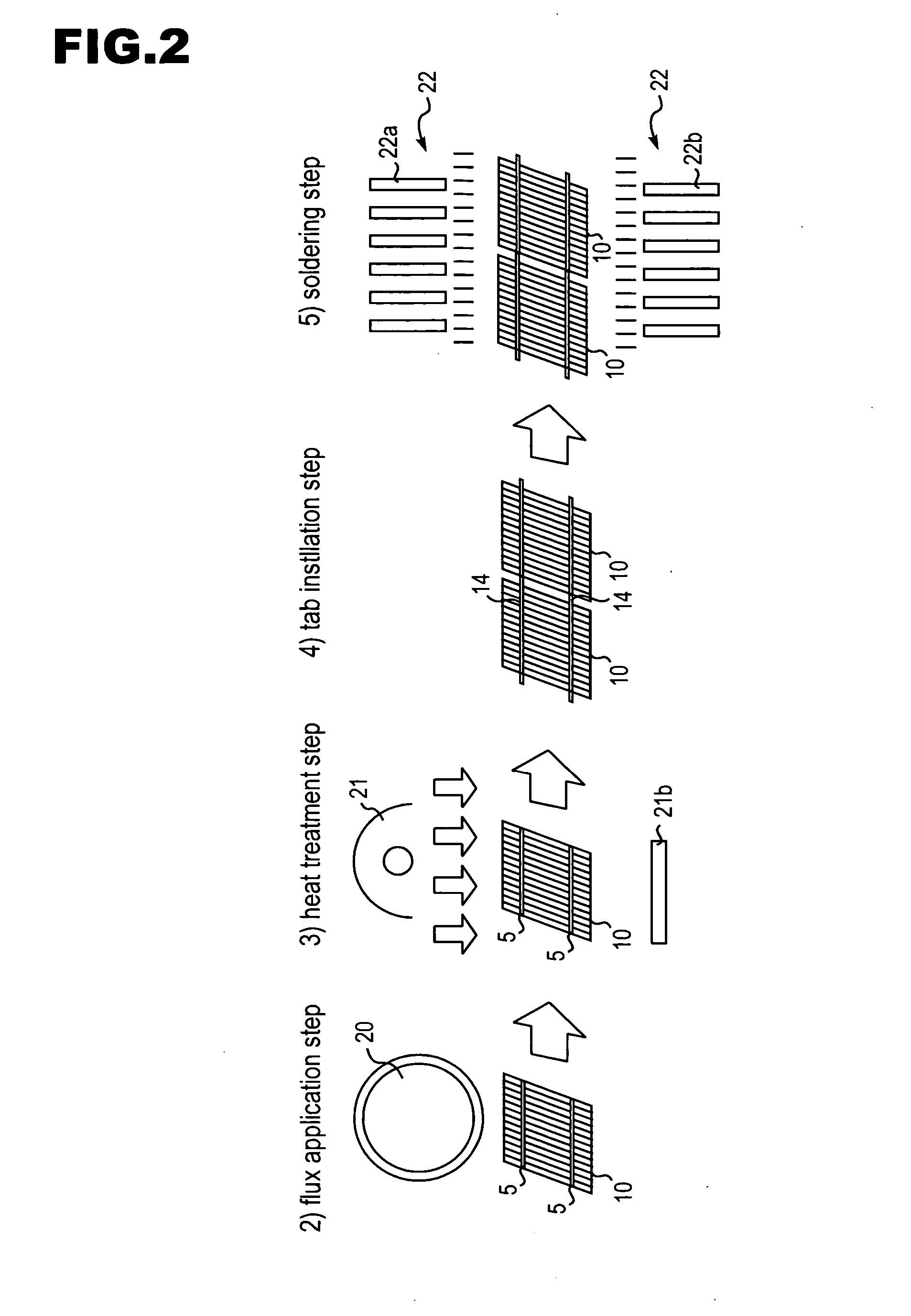
[0049] With reference to the drawings, detailed descriptions will be made on an embodiment of the present invention. Components identical or equivalent to each other in the drawings are denoted the same reference number, and will not be further explained to avoid repetition.
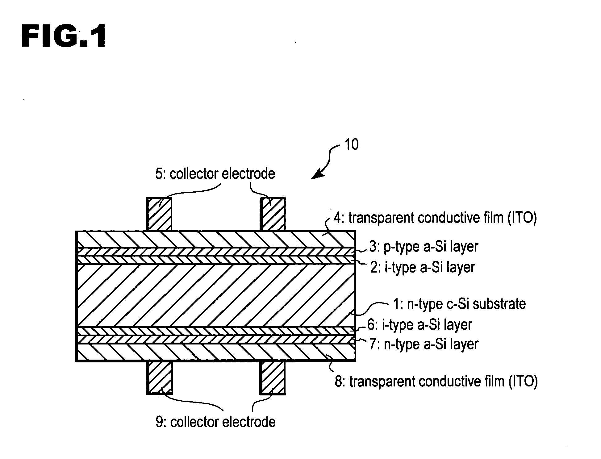
[0050] Firstly, an example of the solar cell to which this invention is applied will be described by referring to FIG. 1. The solar cell 10, as shown in FIG. 1, includes an n-type single-crystal silicon substrate 1 having a thickness of 100 μm to 300 μm and (100) planes (hereinafter referred to as “n-type single-crystal silicon substrate 1) as a crystalline semiconductor substrate. On the surface of the n-type single-crystal silicon substrate 1, there formed pyramidal projections and depressions having a height of a few micro meters to a few tens of micro meters for confining light. A substantially intrinsic i-type amorphous silicon (a-Si:H) layer 2 having a thickness of a few nanometers to a few tens of nanomet...
PUM
 Abstract
Description
Claims
Application Information
 - R&D
- Intellectual Property
- Life Sciences
- Materials
- Tech Scout
- Unparalleled Data Quality
- Higher Quality Content
- 60% Fewer Hallucinations
Browse by: Latest US Patents, China's latest patents, Technical Efficacy Thesaurus, Application Domain, Technology Topic, Popular Technical Reports.
© 2025 PatSnap. All rights reserved.Legal|Privacy policy|Modern Slavery Act Transparency Statement|Sitemap|About US| Contact US: help@patsnap.com


