Nanoelectronic sensor system and hydrogen-sensitive functionalization
a sensor system and electromechanical technology, applied in nanoinformatics, instruments, chemical methods analysis, etc., can solve the problems of limited concentration response, limited industrial use of solid-state chemosensors, and low power of chemical/biomolecular sensors, and achieve the effect of reducing distortions in channel current measuremen
- Summary
- Abstract
- Description
- Claims
- Application Information
AI Technical Summary
Benefits of technology
Problems solved by technology
Method used
Image
Examples
example b
5. EXAMPLE B
Nanotube Network H2 Sensor with Remote Measurement Circuitry
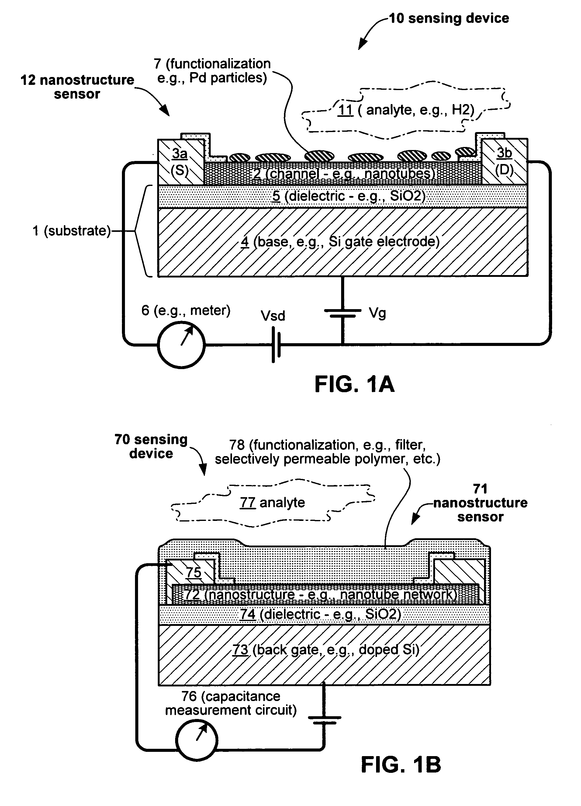
[0118] An exemplary NTFET sensor with measurement circuitry having aspects of the invention may be made as follows. A degenerately doped silicon wafer with a silicon oxide film may be coated with carbon nanotubes in a random network, as described in the above incorporated U.S. patent application Ser. No. 10 / 177,929. As shown schematically in FIG. 9, titanium contacts 35 nm thick covered with gold contacts 100 nm thick were deposited and patterned by photolithography and lift-off to form opposing contacts 100, 110. Contacts 100, 110 each comprised a plurality of interdigitated portions disposed over a generally rectangular region 300. A network of randomly oriented nanotubes 200 is disposed over the silicon substrate. Nanotubes in the network 200 are in electrical contact with interdigitated portions of contacts 100, 110.
[0119] After the deposition of the contacts 102, nanotubes outside of the generally rectang...
example c
6. EXAMPLE C
Passivated / Encapsulated H2 Sensor
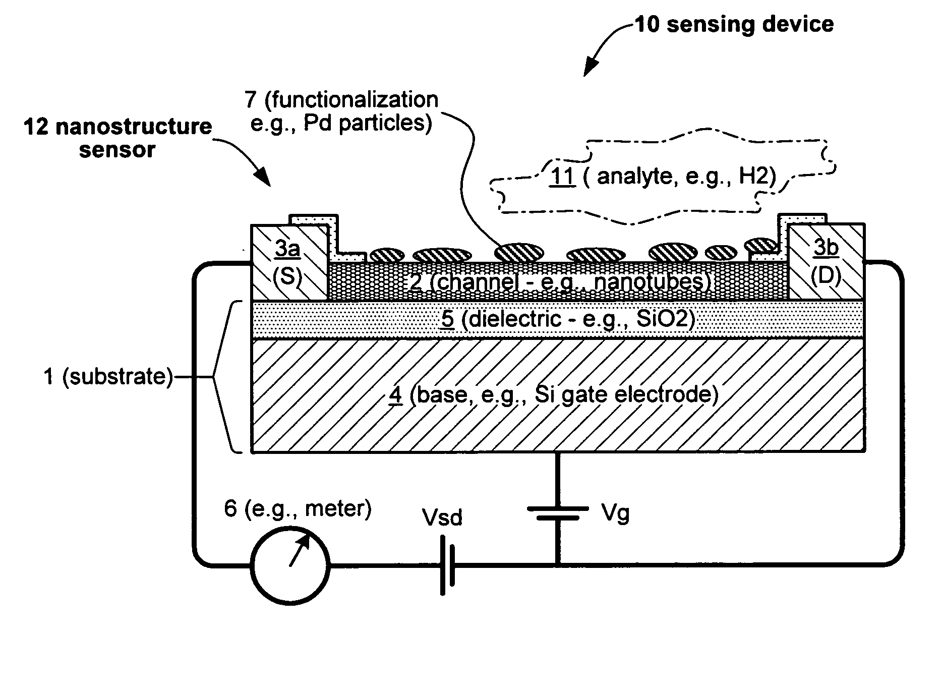
[0128]FIG. 14 shows schematically in cross section an exemplary sensor device 30 having aspects of the invention made using the methods described above. The sensing device 30 includes a nanostructure sensor 37 which makes use of an insulating substrate 31 which may comprise a dielectric material, such as fused quartz and the like.
[0129] The employment of a dielectric substrate material provides electrical isolation of the channel 32 and source and drain contacts 33a, 33b. Optionally, a separate dielectric layer or other electrical isolation element may be included (not shown). In the embodiment of Example A, the channel 32 comprises a carbon nanotube network grown by CVD directly upon the substrate 31 by the methods described above. Optionally, a conditioned surface layer can be included to favor nanotube growth. Alternatively, the channel 32 may be formed of alternative materials and methods as described above.
[0130] In the embodiment...
PUM
 Abstract
Description
Claims
Application Information
 - R&D
- Intellectual Property
- Life Sciences
- Materials
- Tech Scout
- Unparalleled Data Quality
- Higher Quality Content
- 60% Fewer Hallucinations
Browse by: Latest US Patents, China's latest patents, Technical Efficacy Thesaurus, Application Domain, Technology Topic, Popular Technical Reports.
© 2025 PatSnap. All rights reserved.Legal|Privacy policy|Modern Slavery Act Transparency Statement|Sitemap|About US| Contact US: help@patsnap.com


