Multi-bit nonvolatile ferroelectric memory device having fail cell repair circuit and repair method thereof
- Summary
- Abstract
- Description
- Claims
- Application Information
AI Technical Summary
Benefits of technology
Problems solved by technology
Method used
Image
Examples
Embodiment Construction
[0019] The present invention will be described in detail with reference to the accompanying drawings. Wherever possible, the same reference numbers will be used throughout the drawings to refer to the same or like parts.
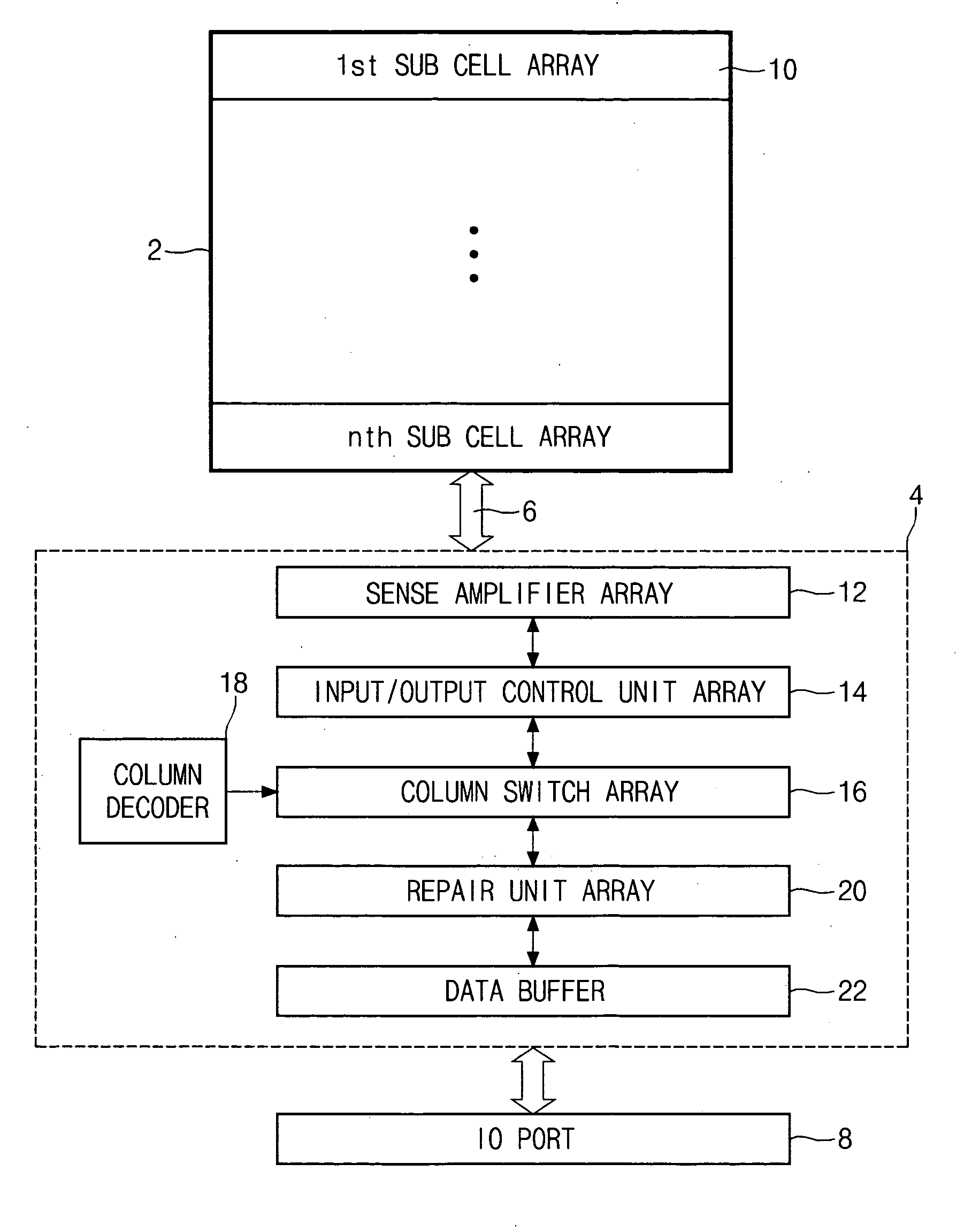
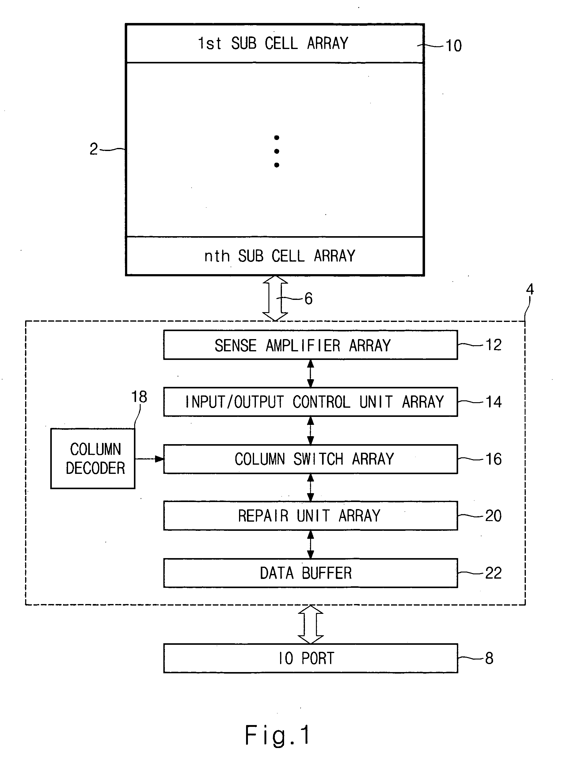
[0020]FIG. 1 is a block diagram illustrating a multi-bit nonvolatile ferroelectric memory device according to an embodiment of the present invention.
[0021] In this embodiment, a multi-bit nonvolatile ferroelectric memory device comprises a cell array block 2, a failed cell repair block 4, a data bus 6, and an input / output port 8.
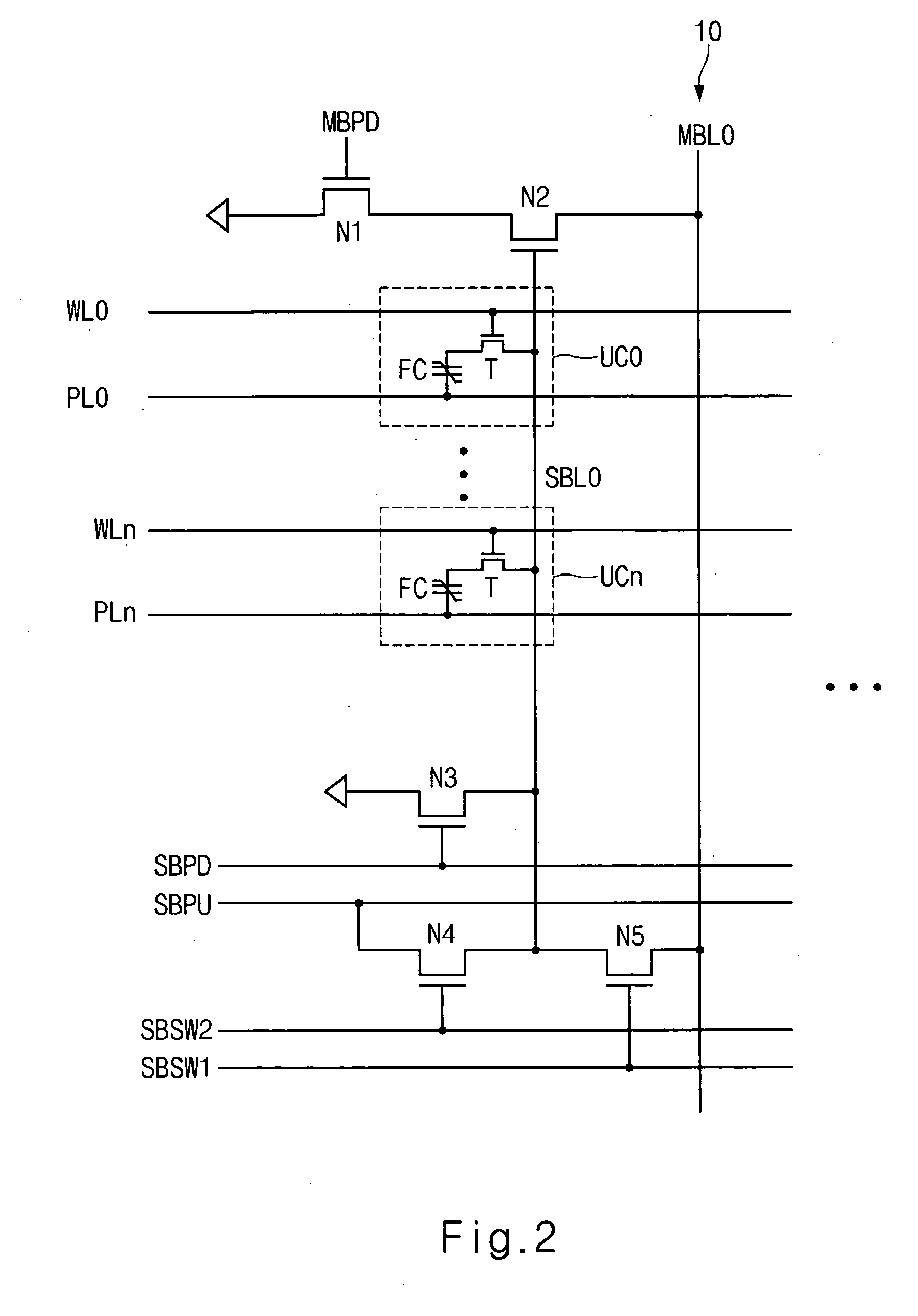
[0022] The cell array block 2 comprises a plurality of sub cell arrays 10. Each of the sub cell arrays 10 has a hierarchical bit line structure including a plurality of sub bit lines SBL connected to one main bit line MBL.
[0023] The failed cell repair block 4 comprises a sense amplifier array 12, an input / output control unit array 14, a column switch array 16, a column decoder 18, a repair unit array 20 and a data buffer 22.
[0024] The se...
PUM
 Abstract
Description
Claims
Application Information
 - R&D
- Intellectual Property
- Life Sciences
- Materials
- Tech Scout
- Unparalleled Data Quality
- Higher Quality Content
- 60% Fewer Hallucinations
Browse by: Latest US Patents, China's latest patents, Technical Efficacy Thesaurus, Application Domain, Technology Topic, Popular Technical Reports.
© 2025 PatSnap. All rights reserved.Legal|Privacy policy|Modern Slavery Act Transparency Statement|Sitemap|About US| Contact US: help@patsnap.com


