
TFT fabrication process

a fabrication process and technology of thin film transistors, applied in the field of tft fabrication process, can solve the problems of low cost of silicon-based thin film transistor circuits, low interest in and insufficient attention to other material components such as dielectric materials

Active Publication Date: 2006-10-19
XEROX CORP
View PDF47 Cites 25 Cited by
  • Summary
  • Abstract
  • Description
  • Claims
  • Application Information

AI Technical Summary

Problems solved by technology

Thin film transistor circuits using current mainstream silicon technology may be too costly, particularly for large-area device applications such as backplane switching circuits for displays like active matrix liquid crystal monitors or televisions, where high switching speeds are not essential.
The high costs of silicon-based thin film transistor circuits are primarily due to the capital-intensive fabrication facilities and the complex high-temperature, high-vacuum photolithographic fabrication processes under strictly controlled environments.
On the other hand, other material components such as dielectric materials have not been receiving much attention.
An issue with conventional gate dielectrics is that it may be difficult to accommodate all the desired attributes for the dielectric materials.

Method used


Image

  • TFT fabrication process
  • TFT fabrication process
  • TFT fabrication process

Examples


example 1

[0082] In this example, poly(vinyl phenol) (Aldrich, Mw=20,000) was used as an electrically insulating material for the second layer, and poly(methyl silsesquioxane) was used as the material for the first layer. A polythiophene having the following formula was used as the semiconductor:

[0083] where n is a number of from about 5 to about 5,000. This polythiophene and its preparation are described in Beng Ong et al., US Patent Application Publication No. US 2003 / 0160230 A1, the disclosure of which is totally incorporated herein by reference.

[0084] Poly(methyl silsesquioxane) was prepared using methyltrimethoxysilane as precursor according to the following procedure. A mixture of 0.88 grams of aq. 0.1 wt % hydrochloric acid solution and 5.13 grams of tetrahydrofuran was added dropwise to a mixture of 4.08 grams of methyltrimethoxysilane and 9.24 grams of methylisobutylketone in a 3-necked flask cooled with an ice bath over a period of 30 minutes with rigorous stirring under a dry at...

example 2

[0089] In this example, poly(methyl silsesquioxane) was used for the first layer while poly(4-vinylphenol-co-methyl methacrylate) was used for the second layer. Bottom-gate, top-contact OTFTs were fabricated using the same procedure as in Example 1. Thin film transistors with channel lengths of about 60 microns and channel widths of about 1000 microns were used for evaluation. The devices showed field-effect mobility of 0.12 cm2 / V·s and a current on / off ratio of 1.5×10⁵.

example 3

[0090] The preparation of methyl silsesquioxane / zirconium oxide hybrid composition is shown in Scheme 1. A mixture of 0.88 grams of aq. 0.1 wt % hydrochloric acid and 5.13 grams of tetrahydrofuran was added dropwise to a mixture of 4.08 grams of methyltrimethoxysilane and 10 grams of methylisobutylketone in a 3-necked flask cooled with an ice bath with vigorous stirring under a dry atmosphere. The mixture was allowed to warm to room temperature and then heated to 60° C. for 3 hours. Subsequently, a mixture of 80 wt % 6.166 grams of zirconium butoxide and 12.8 grams of tetrahydrofuran was added dropwise over a period of 30 minutes. After addition of 18.0 grams of tetrahydrofuran, the mixture was stirred at 60° C. for 3 hours and then cooled to room temperature before being used in fabricating the dielectric layer.

[0091] Bottom-gate, top-contact OTFTs were fabricated using the same procedure as in Example 1. Poly(vinyl phenol) was used for the second layer, and the methyl silsesquio...


PUM

PropertyMeasurementUnit
thicknessaaaaaaaaaa
thicknessaaaaaaaaaa
thicknessaaaaaaaaaa

Abstract

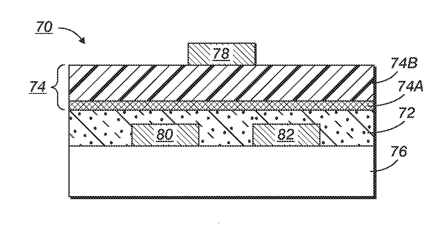
A process for fabricating a thin film transistor including: (a) depositing a semiconductor layer; and (b) depositing a multilayer gate dielectric prior to or subsequent to the depositing the semiconductor layer, wherein the multilayer dielectric comprises: (i) a first layer comprising a first material selected from the group consisting of an optionally substituted silsesquioxane, an optionally substituted silsesquioxane-metal oxide hybrid composition, an optionally substituted siloxane-metal oxide hybrid composition, and a mixture thereof, and (ii) a second layer in contact with the first layer, wherein the second layer comprises a second material, wherein the first layer is closer to the semiconductor layer than the second layer.

Description

CROSS-REFERENCE TO RELATED APPLICATIONS [0001] This application is a divisional application of co-pending U.S. application Ser. No. 11 / 104,728 (filing date Apr. 13, 2005) from which priority is claimed, the disclosure of which is totally incorporated herein by reference. [0002] Yiliang Wu et al., U.S. application Ser. No. 10 / 982,472, filed Nov. 5, 2004, titled DIELECTRIC MATERIALS FOR ELECTRONIC DEVICES (Attorney Docket No. A3392-US-NP), the disclosure of which is totally incorporated herein by reference. [0003] Yiliang Wu et al., U.S. application Ser. No. 11 / 104,730, filed Apr. 13, 2005, titled TFT GATE DIELECTRIC WITH CROSSLINKED POLYMER (Attorney Docket No. 20040952-US-NP), the disclosure of which is totally incorporated herein by reference.STATEMENT REGARDING FEDERALLY SPONSORED RESEARCH OR DEVELOPMENT [0004] This invention was made with United States Government support under Cooperative Agreement No. 70NANBOH3033 awarded by the National Institute of Standards and Technology (NI...

Claims


Application Information

Patent Timeline
Patent Type & Authority Applications(United States)
IPC IPC(8): H01L21/84H01L21/31
CPCH01L29/513H01L51/0036H01L51/0097H01L51/0545H01L51/0529H01L51/0537H01L51/0541H01L51/052H10K85/113H10K10/471H10K10/474H10K10/478H10K10/464H10K10/466H10K77/111
Inventor LIU, PINGWU, YILIANGONG, BENGS
Owner XEROX CORP
Learn More