
Display driver and display driving method

Inactive Publication Date: 2006-10-12
RENESAS ELECTRONICS CORP
View PDF6 Cites 16 Cited by
  • Summary
  • Abstract
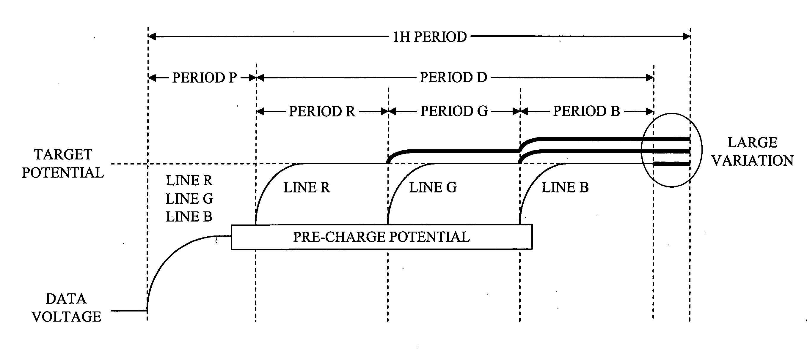
  • Description
  • Claims
  • Application Information

AI Technical Summary

Benefits of technology

[0006] Accordingly, an object of the present invention is to provide a display driver, which can reduce a holding potential fluctuation of a data line without adding any new circuit and without depending on a display pattern.
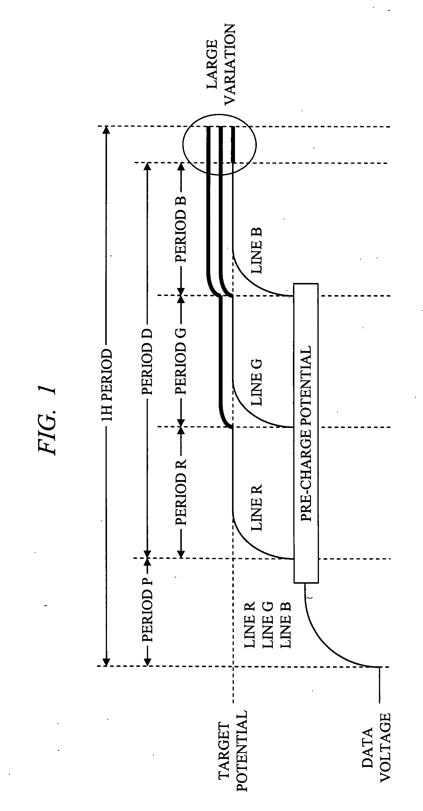
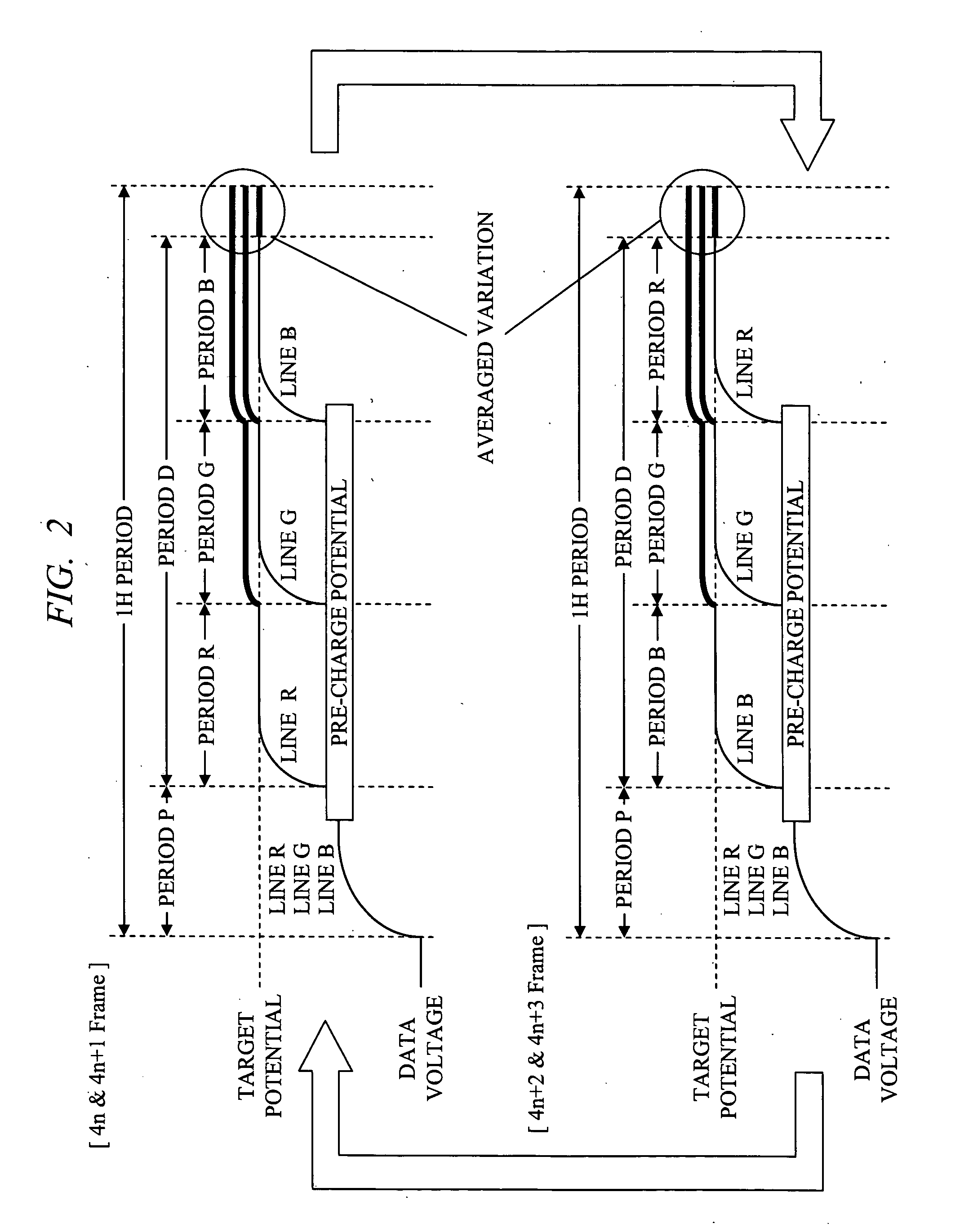
[0007] As mentioned above, for the reduction of the fluctuation of the holding potential of the data line in the floating state, it is effective to average and reduce the fluctuation amount of the holding potential. That is to say, if the fluctuation in the holding potential can be averaged and reduced, the problem of the fluctuation in the holding potential can be solved. Paying attention to this point, in the display driver of the present invention, the period D following the period P in one scanning period is divided into a period R, a period G, and a period B in which data voltage is applied to the data lines R, G, and B, respectively. The output order of the data voltage in the period D is switched in each two frames between the order of period R→period G→period B and the order of period B→period G→period R, and different output orders of data voltages are set in each of adjacent pixels on the display panel so as to form the checkerboard display pattern. By doing so, the degradation in picture quality can be prevented and the fluctuations in the holding potentials of the data lines R, G, and B can be averaged, so that the fluctuation amount can be reduced to half. Accordingly, the problem of the fluctuation in the holding potential can be solved.
[0008] According to the present invention, the fluctuation in the holding potential can be averaged and reduced in all the data lines only by changing the output operation of the data voltages in time-sharing drive. Therefore, it is possible to provide a display driver capable of reducing the fluctuation in the holding potential of the data lines without newly adding any circuit and without depending on the display pattern.

Problems solved by technology

However, in the method described in Japanese Patent Application Laid-Open Publication No. 2004-191544 mentioned above, since it is necessary to newly add a circuit for calculating the average value of the data voltages; there is a problem that a circuit scale is increased.
Further, since such a case may occur where a data voltage largely deviated from the average value is applied depending on a display data, there is a problem that a display pattern dependency affects the effect of reducing the holding potential fluctuation.

Method used


Image

  • Display driver and display driving method
  • Display driver and display driving method
  • Display driver and display driving method

Examples


first embodiment

[0031] The configuration and operation of the display driver according to a first embodiment of the present invention will be described below with reference to FIG. 4 to FIG. 9.

[0032] First, FIG. 4 shows a block configuration of a display driver according to the first embodiment of the present invention. In FIG. 4, a reference numeral 101 denotes a drive circuit, 102 denotes a system interface (IF), 103 denotes a register, 104 denotes a memory controller, 105 denotes a display memory, 106 denotes a timing generator, 107 denotes a multiplexer (MUX), 108 denotes a reference voltage generator, 109 denotes a data voltage generator, 110 denotes a data voltage selector (64 to 1), 111 denotes an operational amplifier (Op-AMP), 112 denotes a demultiplexer (DeMUX), 113 denotes a scanning line driver, 114 denotes a display panel, and 115 denotes a CPU.

[0033] The drive circuit 101 is a so-called display memory built-in type controller driver, and it includes achieving means according to the ...

second embodiment

[0056] Next, a display driver according to a second embodiment of the present invention will be described below with reference to FIG. 10 and FIG. 11. FIG. 10 shows a pattern displayed by outputting the voltages in the different orders to each two pixels adjacent in the vertical direction (hereinafter referred to as “each-two-dots toggle pattern”). Note that the display driver of this embodiment has the same configuration as that of the first embodiment of the present invention shown in FIG. 4 to FIG. 8.

[0057] For example, in the FRC (frame rate control) in which the number of grayscales is increased in a pseudo way by producing intermediate colors by displaying two colors with difference in luminance while switching them in each frame, a checkerboard pattern is used as a display pattern in order to increase the spatial frequency similar to the first embodiment. In this case, in the first embodiment of the present invention, due to the synchronization with the FRC, difference in br...

third embodiment

[0063] Next, a display driver according to a third embodiment of the present invention will be described below with reference to FIG. 12. FIG. 12 shows a pattern displayed by switching the each-one-dot toggle pattern in each four frames.

[0064] For example, in the above-mentioned FRC, display patterns may be switched in each two frames so as to remove the DC current in both of the active and positive polarities. For this reason, in the toggle method shown in the first embodiment, due to the synchronization with the FRC, DC components probably remain, and as a result, the degradation in a liquid crystal element may occur. Thus, the display pattern is switched in each four frames so as to prevent the interference with that in which display patterns are switched in each two frames such as both of the positive and negative polarities and the FRC.

[0065] Note that, with respect to the operation timing, the operation timing of SRA and SRB and that of SBA and SBB shown in the first embodim...


PUM


Abstract

In a display driver, a period D following a period P in one scanning period is divided into periods R, G, and B in which data voltages are applied to data lines R, G, and B, and two output orders of the data voltage such as the period R→the period G→period B and the period B→the period G→period R are switched in each two frames.

Description

CROSS-REFERENCE TO RELATED APPLICATION [0001] The present application claims priority from Japanese Patent Application No. JP 2005-85170 filed on Mar. 24, 2005, the content of which is hereby incorporated by reference into this application. TECHNICAL FIELD OF THE INVENTION [0002] The present invention relates to a display driver for an active matrix display using a TFT (Thin Film Transistor) liquid crystal or the like. More particularly, it relates to a technology effectively applied to a driving method and a drive circuit which can reduce a fluctuation of data voltage held in a data line, in a drive system in which the data voltage is outputted in a time-sharing manner in one horizontal period. BACKGROUND OF THE INVENTION [0003] In general, in the active matrix display in which a plurality of scanning lines and a plurality of data lines are arranged in a matrix shape, a scanning voltage showing a selected state is sequentially applied to the scanning line in each one scanning perio...

Claims


Application Information

Patent Timeline
IPC IPC(8): G11C7/06
CPCG09G3/20G09G3/3688G09G2310/0235G09G2320/0209G09G2310/027G09G2310/0297G09G2310/0248G09G3/36
Inventor ERIGUCHI, TAKUYAKUDO, YASUYUKIAKAI, AKIHITOTAKADA, NAOKISAKAMAKI, GORO
Owner RENESAS ELECTRONICS CORP
Learn More