Contacting device, testing method and corresponding production method
a technology of contacting device and production method, which is applied in the direction of semiconductor devices, semiconductor/solid-state device details, instruments, etc., can solve the problems of high testing cost, high cost of testing, and commercial disadvantages, and achieve the effect of reliable low-impedance temporary electrical conta
- Summary
- Abstract
- Description
- Claims
- Application Information
AI Technical Summary
Benefits of technology
Problems solved by technology
Method used
Image

Examples
first embodiment
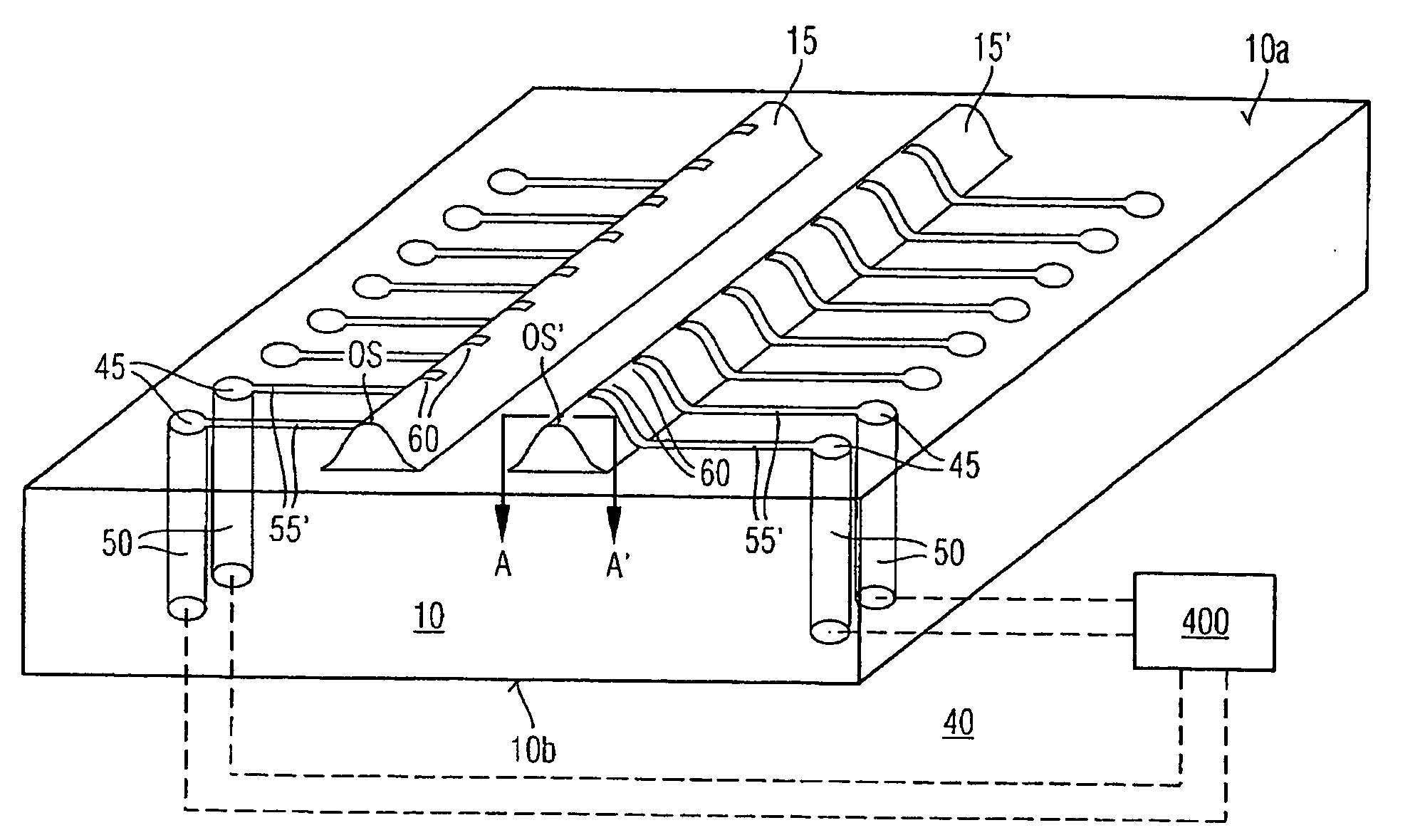
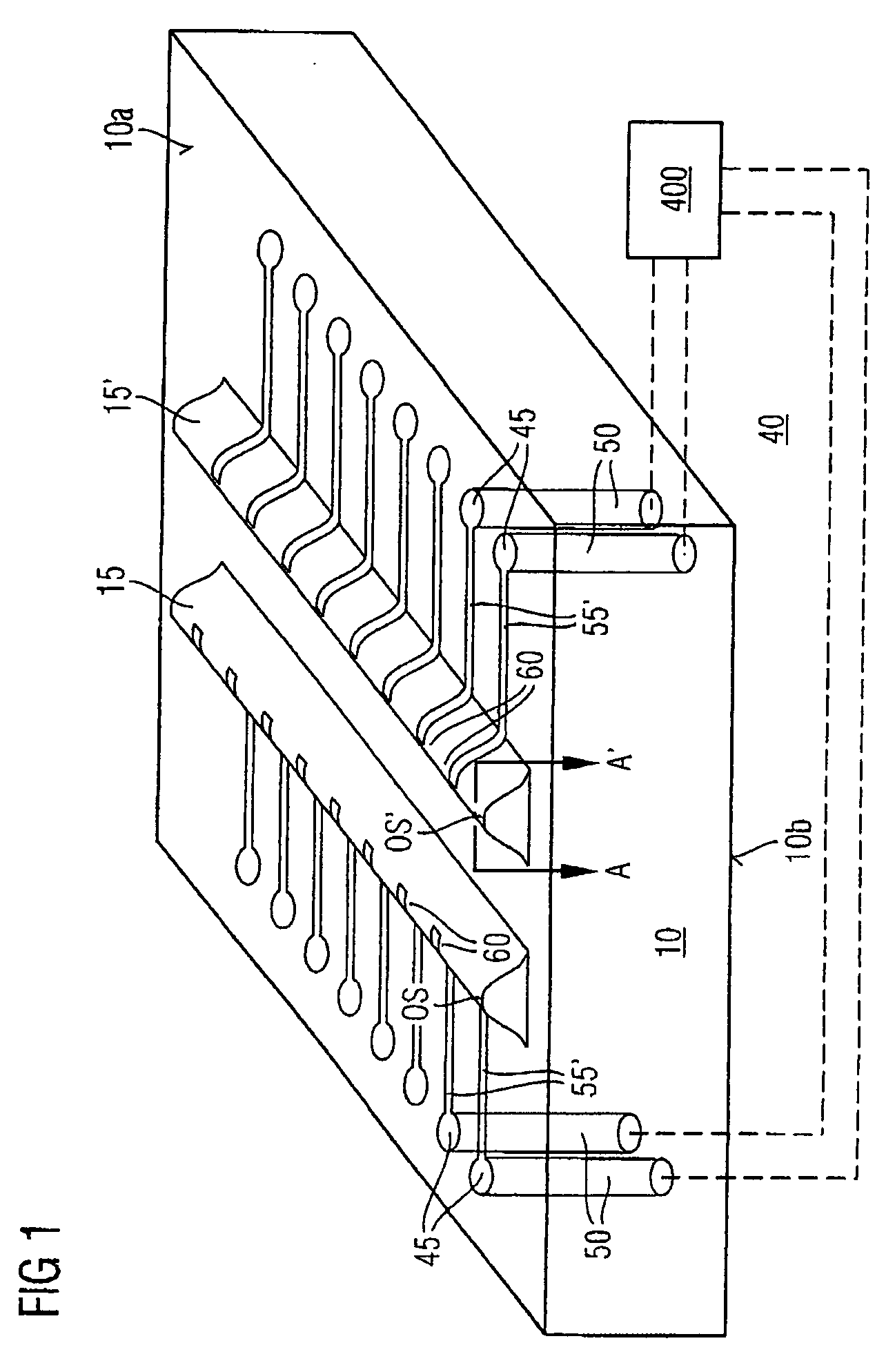
[0028]FIG. 1 is a schematic representation of a contacting device according to the present invention.
[0029] In FIG. 1, reference numeral 10 designates a carrier device of an organic material or of silicon or a ceramic, which has a rectangular form and a first, upper surface 10a and a second, lower surface 1b.
[0030] On the upper surface 10a there are two elastic elevations 15, 15′ of an elastomer, such as for example silicone, polyurethane or flexibilized epoxy. The elastic elevations have an elongate, wall-shaped form and follow in their shape the contact areas to be contacted of the chip to be tested. They may be applied, for example, by a printing process or by dispensing.
[0031] A plurality of first terminal regions 45 are provided on a first surface 10a, to be precise in respective rows parallel to the first and second elastic elevations 15, 15′. Starting from the first terminal regions 45, interconnects 55′ run to the upper side OS and OS′, respectively, of the elastic elevati...
second embodiment
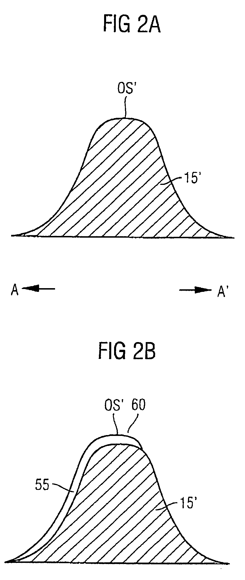
[0040]FIG. 4 is a cross-sectional view of an elastic contact element of a contacting device according to the present invention along the line A-A′ in FIG. 1.
[0041] As shown in the embodiment according to FIG. 4, it is sufficient if such particles 65″ are merely provided on the surface of the elastic elevation 15′.
[0042] The particles 65′ according to FIG. 3 may be mixed into the elastomer before processing. The particles 65″ according to FIG. 4 are applied to the non-cured elastomer surface after processing and remain adhesively attached therein.
[0043] The particles 65′ and 65″, incorporated in or applied to the elastomer of the elastic elevation 15′ according to FIG. 3 and FIG. 4, respectively, are, as mentioned above, molded by the interconnects 55′ and 55″, respectively, and consequently produce in the regions 60 very rough surfaces, which lead to reliable and low-impedance contacting of oxidized contact areas of the integrated circuit 2, 2′ of the chip 1. Hard gold preferably ...
third embodiment
[0044]FIG. 5 is a cross-sectional view of an elastic contact element of a contacting device according to the present invention along the line A-A′ in FIG. 1.
[0045] In the case of the embodiment according to FIG. 5, particles 65′″ are integrated in the interconnect 55′″ and not in the elastic elevation 15′. This may take place by embedding non-conducting or conducting particles 65′″ in an electrodepositing process. Such dispersive, electrolytic depositing is also used for example in the production of grinding wheels. As an alternative to this, the embedding of such particles 65′″ by a currentless depositing process is also possible. When non-conducting particles 65′″ are used, they must be completely embedded; conducting particles 65′″ may also be only partially embedded.
PUM
 Abstract
Description
Claims
Application Information
 - R&D
- Intellectual Property
- Life Sciences
- Materials
- Tech Scout
- Unparalleled Data Quality
- Higher Quality Content
- 60% Fewer Hallucinations
Browse by: Latest US Patents, China's latest patents, Technical Efficacy Thesaurus, Application Domain, Technology Topic, Popular Technical Reports.
© 2025 PatSnap. All rights reserved.Legal|Privacy policy|Modern Slavery Act Transparency Statement|Sitemap|About US| Contact US: help@patsnap.com