
Method of forming film bulk acoustic wave filter assembly

a technology of acoustic wave filter and film, which is applied in the direction of impedence network, electrical apparatus, semiconductor devices, etc., can solve the problems of increasing system integration complexity, and achieve the effect of less complicated system integration and increased resonator characteristics

Active Publication Date: 2006-09-21
NAT CHUNG SHAN INST SCI & TECH
View PDF9 Cites 19 Cited by
  • Summary
  • Abstract
  • Description
  • Claims
  • Application Information

AI Technical Summary

Benefits of technology

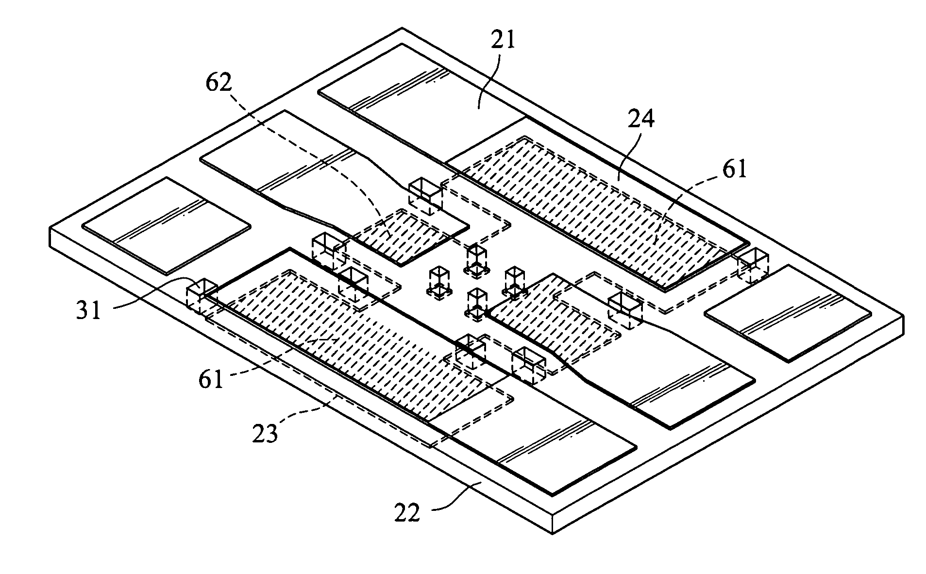
[0005] An object of the invention is therefore to provide a film bulk acoustic wave filter assembly in which a film bulk acoustic wave filter is integrated with an RF circuit as a single chip so that the filter or a duplexer can be designed with circuit design simultaneously. In the invention, less than 2 μm thick piezoelectric film is grown on a silicon chip having active devices thereon, without any need of a piezoelectric chip. Passive device production can be integrated with the semiconductor process of forming a silicon chip having active devices thereon so as to form a suspended piezoelectric film. The piezoelectric film is first grown directly on an integrated circuit silicon chip at a temperature in the tolerable range of the circuit. An under-metal sacrificed layer is then etched off to form the suspended piezoelectric film. Replacement of semiconductor metal is further performed to grow a lower electrode and increase the characteristics of the resonator. Thereby, the simulation design is completed and system integration is less complicated, which has a great influence on integration of active / passive devices and SOC chip production.

Problems solved by technology

The wiring parts of the connection between the passive devices and the RF circuit generate parasitic effects due to RF signals, thereby increasing complexity in system integration.

Method used


Image

  • Method of forming film bulk acoustic wave filter assembly
  • Method of forming film bulk acoustic wave filter assembly
  • Method of forming film bulk acoustic wave filter assembly

Examples


Embodiment Construction

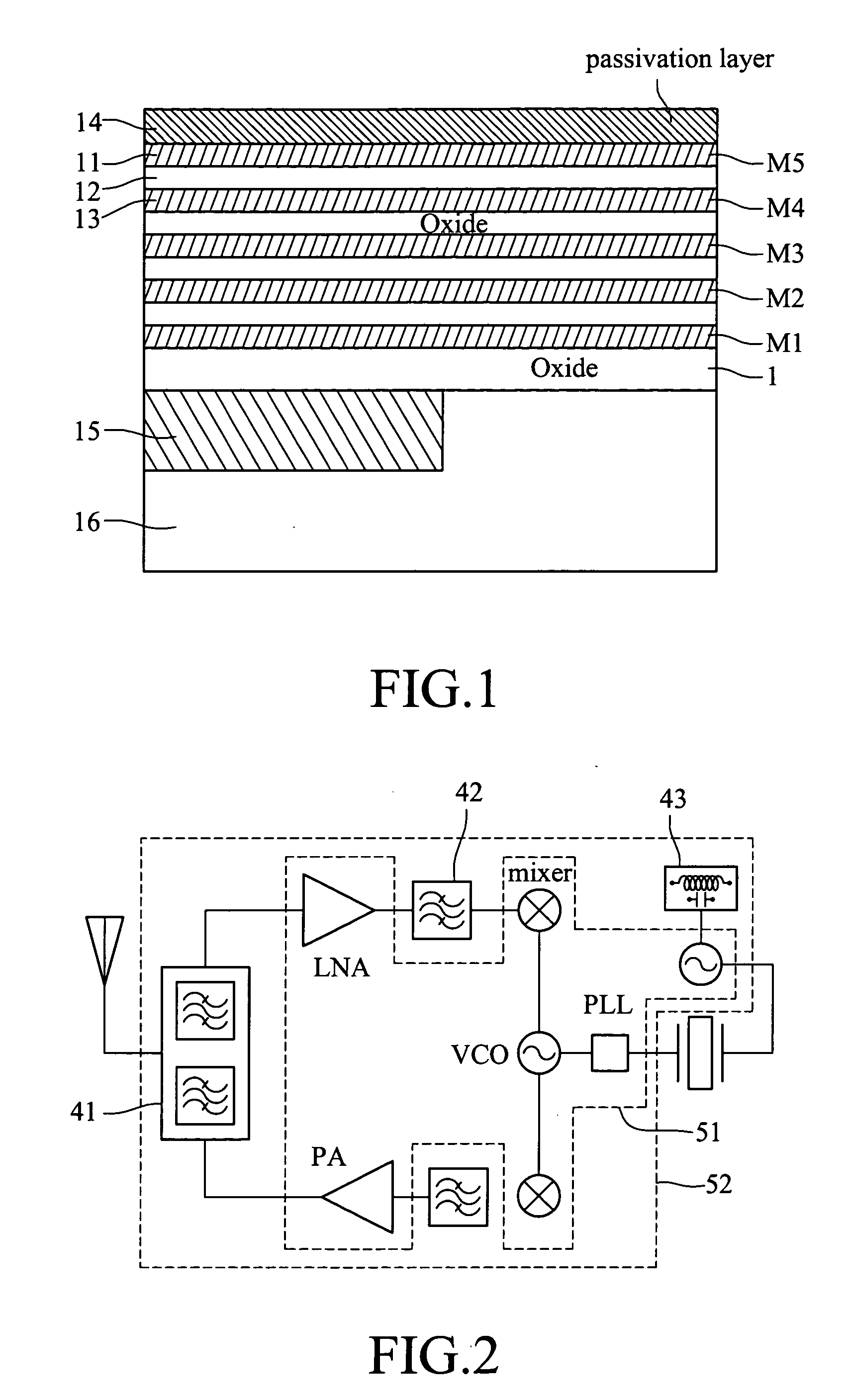
[0012]FIG. 1 is a cross-sectional view of an IC chip obtained from CMOS standard processes. FIG. 2 is a schematic view showing part of the RF circuit region and part of the RF integrated chip of the invention.

[0013] Referring to FIG. 1, there are passivation layer 14, first metal layer 11, first silicon oxide layer 12 and second metal layer 13 successively above the IC chip.

[0014] Referring to FIG. 2, the front end module of conventional CMOS RF integrated circuit includes a low noise amplifier (LNA), a mixer, a voltage control oscillator (VCO) and a phase loop lock, which are able to be integrated on single chip at the beginning of the circuit design. Through the invention, passive devices that used to be produced individually in the art, such as a film bulk acoustic wave duplexer 41, film bulk acoustic filter 42 and film bulk acoustic wave resonator 43, can be produced integrally with an RF active circuit region 51 by a standard process and a silicon micro-electro-mechanical pos...


PUM


Abstract

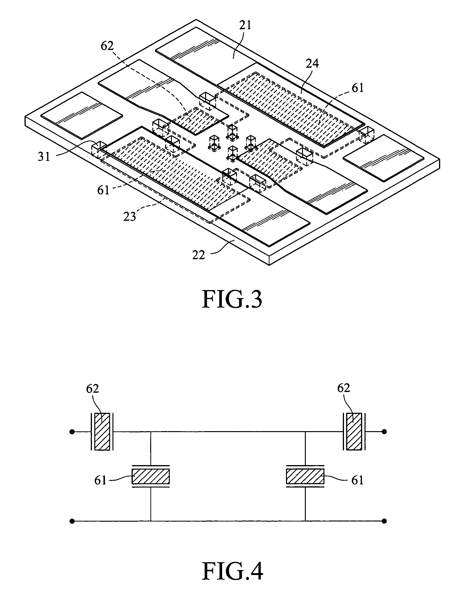
A film bulk acoustic wave filter assembly includes a film bulk acoustic filter and an RF circuit. The film bulk acoustic filter unit cell includes a plurality of film bulk acoustic wave resonators. The number, area and arrangement of the resonators depend on the characteristics of the filter. In the film bulk acoustic wave filter, a metal layer made by CMOS processes is used as a lower electrode area of the film bulk acoustic wave filter or a suspended chamber. The film bulk acoustic filter can be integrated with the RF circuit using processes such as the CMOS process. It facilitates the integration of active devices, streamlining of system design and simplification of test processes, and has a great influence on the application of RF communication devices and integration of system-system-chip (SOC).

Description

BACKGROUND OF THE IVENTION [0001] 1. Field of the Invention [0002] This invention relates to a film bulk acoustic wave filter assembly, and more particularly to a film bulk acoustic wave filter assembly that can be applied in the integration of high-frequency circuit design and SOC. [0003] 2. Related Art [0004] RF micro devices are key aspects of the development of wireless communication. Communication passive devices such as duplexers, filters and power amplifiers need to be combined with an RF circuit individually. The wiring parts of the connection between the passive devices and the RF circuit generate parasitic effects due to RF signals, thereby increasing complexity in system integration. For example, U.S. Pat. No. 6,285,866 published on Sep. 4, 2001, discloses high-frequency passive devices and other active / passive devices that are integrated on a single chip to streamline system design and simplify test processes. According to the disclosure a thin or thick piezoelectric cry...

Claims


Application Information

Patent Timeline
IPC IPC(8): H03H9/58
CPCH03H3/02H03H9/0557H03H9/545H03H9/564H03H9/568H03H2003/021Y10S438/956
Inventor SUNG, PO-HSUNCHEN, PEI-YENCHIN, YUNG-CHUNGCHANG, PEI-ZENPANG, YEN-MINGFANG, CHI-MINGHOU, CHUN-LI
Owner NAT CHUNG SHAN INST SCI & TECH
Learn More