Magnetic tunnel junction structure with amorphous CoFeSiB or NiFeSiB free layer

a tunnel junction and amorphous technology, applied in the direction of magnetic bodies, galvano-magnetic devices, solid-state devices, etc., can solve the problem of large write currents, and achieve the effect of large tmr ratio and low switching field

Active Publication Date: 2006-09-14
SAMSUNG ELECTRONICS CO LTD
View PDF4 Cites 2 Cited by
  • Summary
  • Abstract
  • Description
  • Claims
  • Application Information

AI Technical Summary

Benefits of technology

[0012] An object of the present invention is to substantially solve at least the above problems and / or disadvantages and to provide at least the advantages below. Accordingly, an object of the present invention is to provide an MTJ structure with a low switching field and a large TMR ratio.

Problems solved by technology

A smaller cell, however, requires a larger switching field (HSW) because a large demagnetizing field arises from the poles of the submicrometer-sized cell edge, leading to large write currents.

Method used


Image

  • Magnetic tunnel junction structure with amorphous CoFeSiB or NiFeSiB free layer
  • Magnetic tunnel junction structure with amorphous CoFeSiB or NiFeSiB free layer
  • Magnetic tunnel junction structure with amorphous CoFeSiB or NiFeSiB free layer

Examples


Embodiment Construction

[0028] Preferred embodiments of the present invention will be described herein below with reference to the accompanying drawings. In the following description, well-known functions or constructions are not described in detail since they would obscure the invention in unnecessary detail.

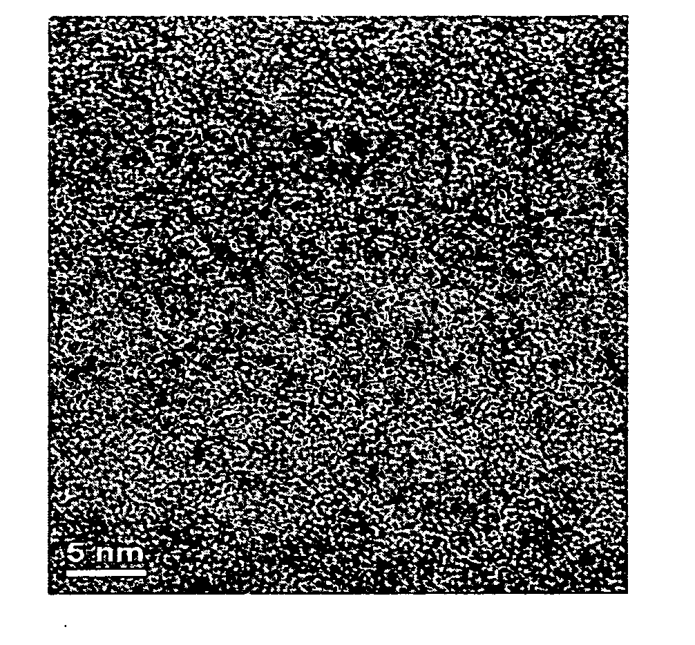
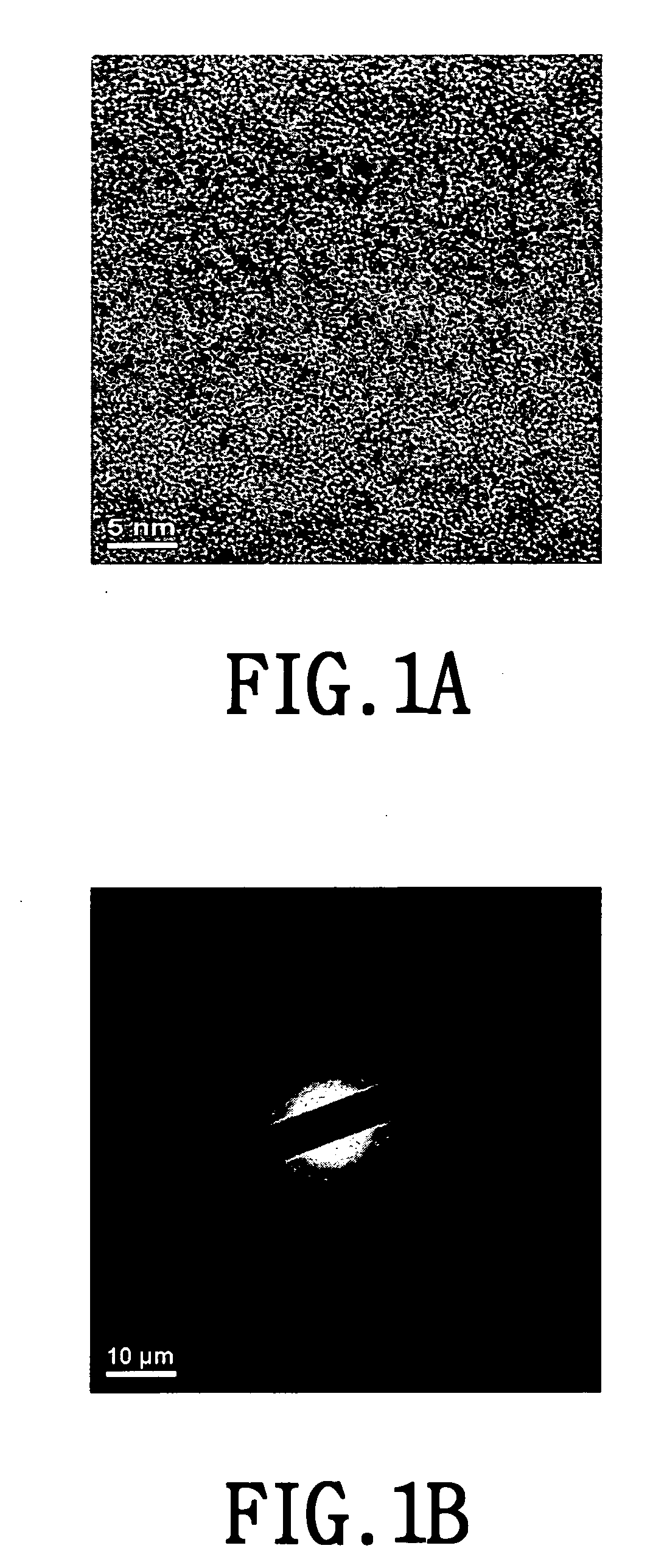
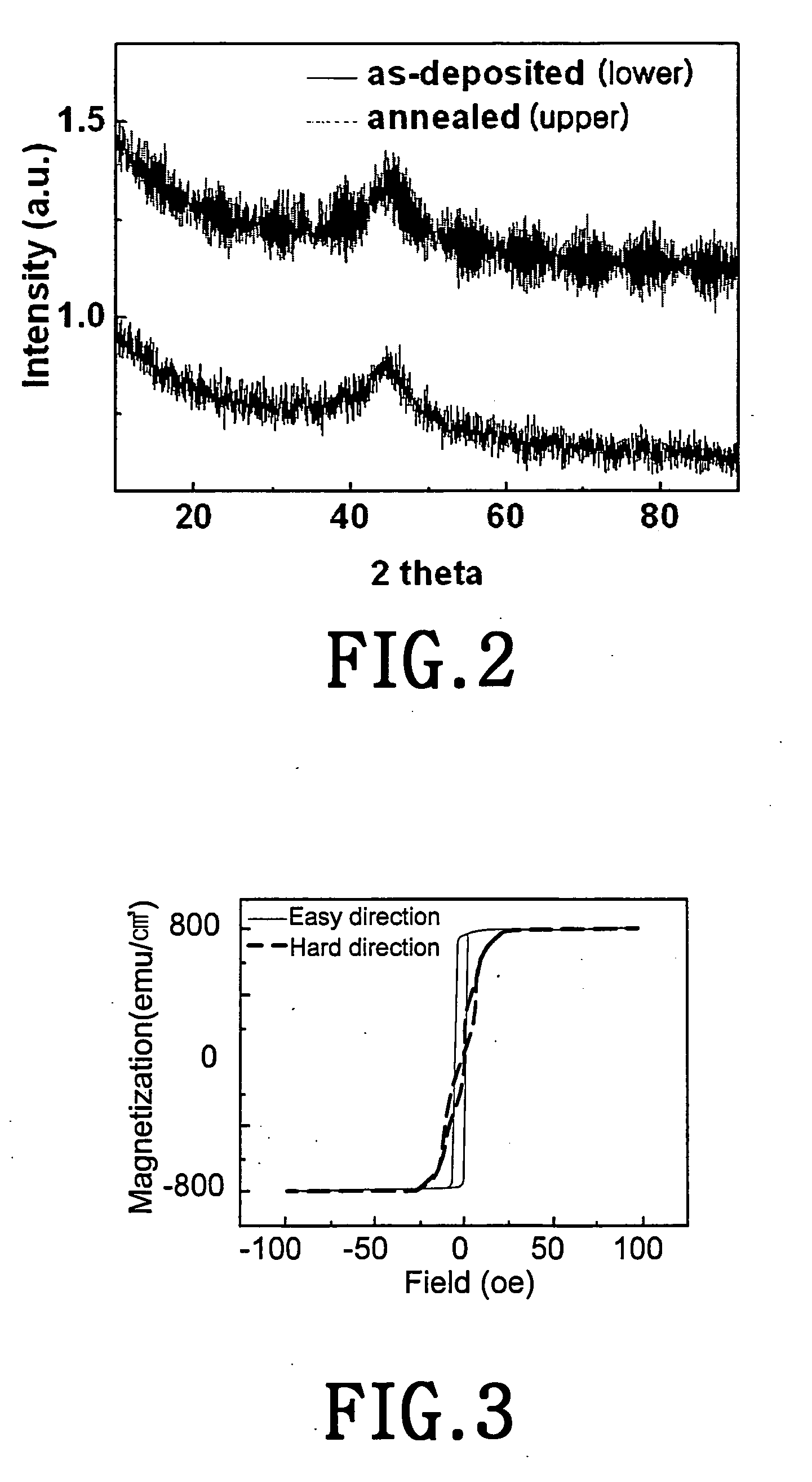
[0029] The present invention is intended to provide an MTJ structure with an amorphous CoFeSiB or NiFeSiB free layer.

[0030] The MTJ structure according to the present invention is a Si / SiO2 / Ta (45 nm) / Ru (9.5 nm) / IrMn (10 nm) / CoFe (7 nm) / AlOx / {CoFeSiB (7 nm) single layer or a CoFeSiB (t nm) / Ru (1.0 nm) / CoFeSiB (7-t nm) synthetic layer} (8.0 nm) / Ru (60 nm) and

[0031] Another structure is a Si / SiO2 / Ta (45 nm) / Ru (9.5 nm) / IrMn (10 nm) / CoFe (7 nm) / AlOx / {NiFeSiB (7 nm) single layer or a NiFeSiB (t nm) / Ru (0.5 nm) / NiFeSiB (7-t nm) synthetic layer} (7.5 nm) / Ru (60 nm).

[0032] That is, a conventional CoFe and / or NiFe layer used as an MTJ free layer is replaced with a CoFeSiB or NiFeSiB free layer.

[0033] In...


PUM


Abstract

A magnetic tunnel junction (MTJ) structure for a magnetic random access memory (MRAM) is provided. Specifically, an MTJ structure with an amorphous CoFeSiB or NiFeSiB free layer is provided. The free layer is a CoFeSiB single layer, a NiFeSiB single layer, a CoFeSiB/Ru/CoFeSiB SAF layer, or a NiFeSiB/Ru/NiFeSiB SAF layer.

Description

PRIORITY [0001] This application claims priority under 35 U.S.C. § 119 to applications entitled “Magnetic Tunnel Junctions Employing Amorphous CoFeSiB Free Layer” filed in the Korean Intellectual Property Office on Mar. 9, 2005 and assigned Serial No. 2005-0019395 and “Magnetic Tunnel Junctions Employing Amorphous NiFeSiB Free Layer” filed in the Korean Intellectual Property Office on Mar. 9, 2005 and assigned Serial No. 2005-0019402, the contents of which are herein incorporated by reference. BACKGROUND OF THE INVENTION [0002] 1. Field of the Invention [0003] The present invention relates generally to a magnetic tunnel junction structure for a magnetic random access memory (MRAM), and in particular, to a magnetic tunnel junction structure with an amorphous CoFeSiB or NiFeSiB free layer. [0004] 2. Description of the Related Art [0005] A magnetic random access memory (hereinafter, referred to as an MRAM) has been used in military applications, such as missiles and spaceships. In addi...

Claims


Application Information

Patent Timeline
Patent Type & Authority Applications(United States)
IPC IPC(8): H01L43/00
CPCB82Y25/00H01F10/3254H01L43/10H10N50/85
Inventor KIM, YOUNG-KEUNCHUN, BYONG-SUNRHEE, JANG-ROHHWANG, JAE-YOUN
Owner SAMSUNG ELECTRONICS CO LTD
Why Eureka
Try Eureka