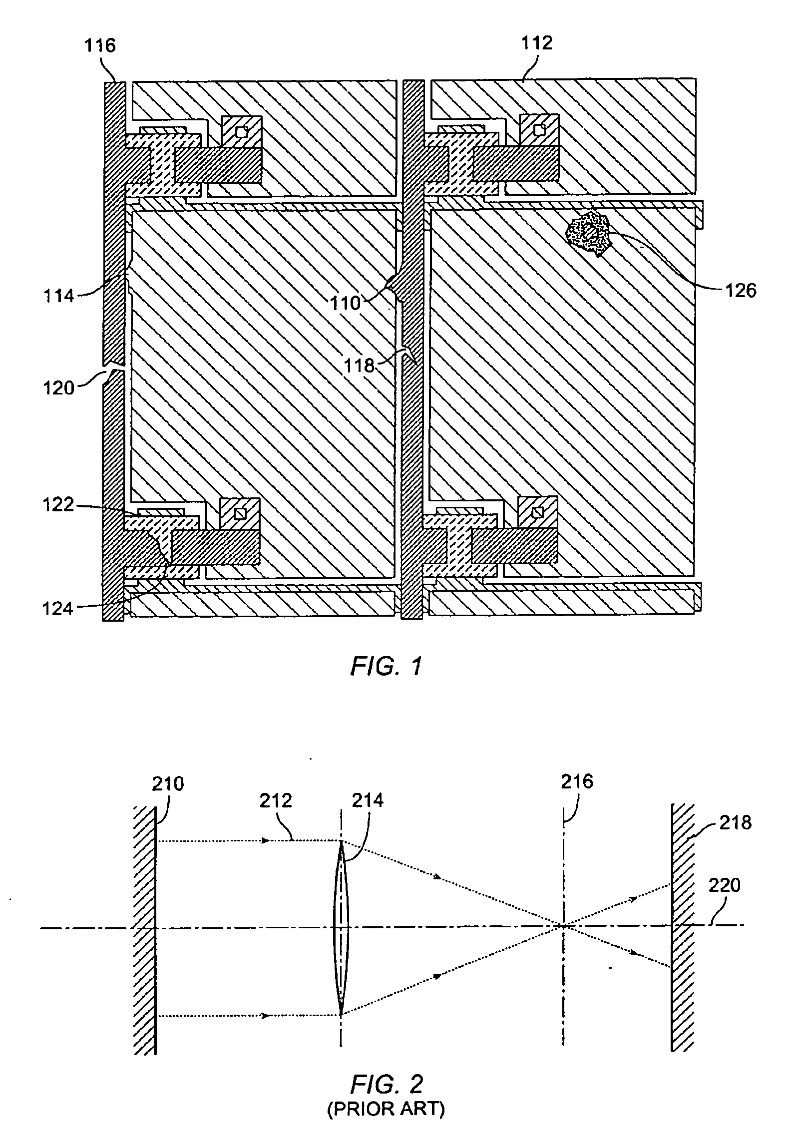
During each of these stages and at various steps within a stage, many production defects may occur, that may have electronic and / or visual implications for the performance of the final LCD product.
Such defects include, but are not limited to: circuit shorts, opens, foreign particles, miss-deposition, feature size problems, and over and under
etching.
In a specific
application domain, such as TFT LCD panel inspection, the article defects subject to detection are small (down to individual micrometers), thus requiring demanding defect detection limits.
However, mere detection of defects is insufficient.
For example, the AOI system resolution can be increased, resulting in improved detection limits (smaller defects detectable); these improvements would, however, have an
adverse effect on the time needed to complete the inspection (tact time) or the system cost.
The inability of the present art to provide high detection sensitivity and tact time matched to the production speed at an acceptable price has imposed on the LCD industry the use of low performance, short tact time systems as in-line instruments.
The operating resolution of an AOI system has a direct
impact on its cost.
For a short tact time, this cost increases almost exponentially with the increase in operating resolution.
Therefore, for high-
throughput, in-line applications at production speeds, where a short tact time is required, only comparatively lower resolutions have been feasible for the system.
Those skilled in the art may recognize that prior
spatial domain image comparison techniques suffer from the
pixelation effect, which always degrades the detection limits of the system.
The
pixelation effect, often interpreted as
noise within an image, becomes especially significant in the vicinity of circuit features where rapid transitions of image intensity occur.
This leads to false detections or masking of legitimate defects.
These effects are highly undesirable since the inspection instruments are expected to have the highest detection sensitivity in the vicinity of TFT array features, such as transistors, data
and gate line crossings.
These methods nevertheless fail to satisfy the demands of this particular
application domain.
The lack of suitable technology to implement an SLM with the required properties has rendered the optical
Fourier filtering principle impractical in the
application domain of interest.
AOI equipment has been characterized by a variety of problems.
If the minimum error over these twenty-five combinations exceeds a threshold value, a defect is assumed.
Hence, they argue that the subsequent sub-pixel interpolation step would do little to improve the detected minimum and a false alignment would result, leading to false alarms in detection.
Although pattern comparison based instruments have been successfully used in the industry for certain applications, the compromise between the system speed (tact time) and accuracy (defect detection limits) has been a
dominant factor imposing what has been considered fundamental limitations.
This ever present compromise for conventional inspection methods limits the usefulness of these systems in the application domain of high-throughput, in-line inspection of large flat patterned media at production speeds, where there is concurrent demand for speed and detection sensitivity.
Despite their inherent limitations, which cause high
false alarm rates or limited sensitivity through relaxed thresholds, conventional
pattern matching techniques have remained the dominant inspection techniques throughout the industry.
However, the emerging application domain of high-throughput in-line optical inspection at production speeds imposes tighter speed and accuracy constraints, which are not achievable by such conventional systems at a practical cost.
Although OFF has been considered to be a candidate to achieve both speed and detection accuracy concurrently, its application has not been considered practical due to a range of problems.
Achieving this type of quality in the past has been impossible except through the use of either static masks (such as photographic films or holographic gratings) or through static or difficult-to-configure mechanical systems.
Static masks remain unsuitable for the presently considered application domain, since the pattern on the material to be inspected often needs to be changed during the regular operation of an AOI instrument and static masks cannot be quickly reconfigured to inspect the object with the new pattern or compensate for the varying orientation of the same pattern.
However, the resulting systems are unacceptably slow to reconfigure.
Moreover, they are constrained with respect to the realizable masking patterns, usually limited to a restricted number of
horizontal and vertical lines.
The use of lines as the masking pattern also causes its own adverse effects, manifesting as parasitic ghosts of defects in the filtered images.
Furthermore, the mechanical implementations of the Fourier filters are complex, costly, unreliable, and unacceptably large in size and, therefore, cannot be easily expanded.
However, the available devices, such as light valves and early forms of transmissive LCDs, could not meet desired performance specifications.
Therefore, these devices were not practical for use in the high-throughput, in-line optical inspection of large flat patterned media at production speeds, while also satisfying industry requirements for detection limits.
Thus, the promise was unfulfilled.


