Nanostructured low-Cr Cu-Cr coatings for high temperature oxidation resistance
a technology of cu-cr coating and nanostructure, which is applied in the direction of vacuum evaporation coating, coating, transportation and packaging, etc., can solve the problems of rapid oxidation at elevated temperatures, corrosion of the combustion chamber lining of the copper-alloy rocket engine, and the use of any of these copper-based materials, so as to achieve enhanced oxidation resistance
- Summary
- Abstract
- Description
- Claims
- Application Information
AI Technical Summary
Benefits of technology
Problems solved by technology
Method used
Image

Examples
example 1
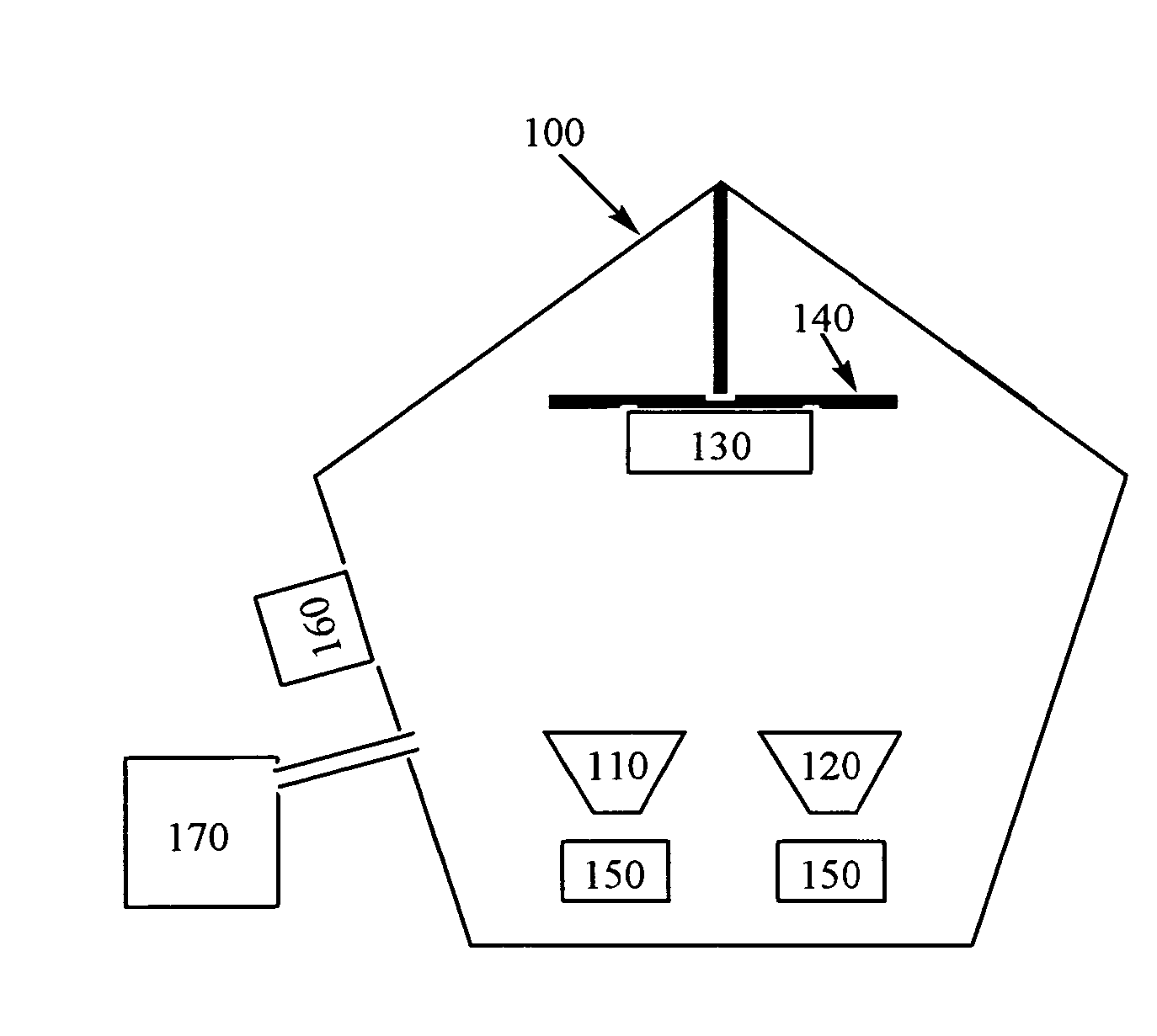
[0034] In one embodiment of the alternating deposition process described above, a substrate 130 consisting of GRCop-84 (Cu-8 atom % Cr-4 atom % Nb) was secured in substrate holder 140. The vacuum chamber 100 was pumped down to below about 5×10⁻⁵ torr with vacuum source 170. Before deposition was commenced, the substrate surface was sputter cleaned for 10 minutes using 75 watt Ar+ ion at 2 KeV. One electron beam source 150 directed at metal source 110 was activated utilizing a beam voltage of 8.0 KeV. Substantially simultaneously, one ion beam source 160 was activated and a beam of ions produced thereby was directed at substrate 130 from an angle of about 45 degrees thereto. The ion beam was generated at 75 W (20 mA, 2 KeV), and consisted of 2.5 sccm poly cold (−63.1° C.) Ar+ ions. A layer of copper (about 100 nm) was deposited thereby onto substrate 130. Thereafter, the activated electron beam source 150 was deactivated and a second ion beam source 150, directed at metal source 120,...
example 2
[0036] In one embodiment of the co-deposition process described above, a substrate 130 consisting of GRCop-84 (Cu-8 atom % Cr-4 atom % Nb) was secured in substrate holder 140. The vacuum chamber 100 was pumped down to below about 5.5×10⁻⁵ torr with vacuum source 170. Before deposition was commenced, the substrate surface was sputter cleaned for 15 minutes using 100 watt Ar+ ion at 2 KeV. Two electron beam sources 150, utilizing a beam voltage of 7.5 KeV each, were activated and directed separately at metal sources 110 and 120, whereupon the copper metal and chromium metal, respectfully, contained therein was thermally evaporated within the chamber 100. Substantially simultaneously, one ion beam source 160 was activated and a beam of ions produced thereby was directed at substrate 130 from an angle of about 45 degrees thereto. The ion beam was generated at 100 W (20 mA, 2 KeV), and consisted of 2.8 sccm poly cold (−63.1° C.) Ar+ ions. The deposition of Cu and Cr was controlled whereb...
PUM
| Property | Measurement | Unit |
|---|---|---|
| diameter | aaaaa | aaaaa |
| total thickness | aaaaa | aaaaa |
| total thickness | aaaaa | aaaaa |
Abstract
Description
Claims
Application Information
 - R&D
- Intellectual Property
- Life Sciences
- Materials
- Tech Scout
- Unparalleled Data Quality
- Higher Quality Content
- 60% Fewer Hallucinations
Browse by: Latest US Patents, China's latest patents, Technical Efficacy Thesaurus, Application Domain, Technology Topic, Popular Technical Reports.
© 2025 PatSnap. All rights reserved.Legal|Privacy policy|Modern Slavery Act Transparency Statement|Sitemap|About US| Contact US: help@patsnap.com