Circuit substrate structure and circuit apparatus

a circuit substrate and circuit technology, applied in the field of circuit substrate structure, can solve the problems of variation in the operating performance of the circuit substrate structure, adverse effects on the operation performance of a nearby circuit, and interference with the incorporation of printed electric components, etc., to suppress electromagnetic leakage from coil patterns, stabilize performance, and suppress the effect of electromagnetic leakag

Inactive Publication Date: 2006-08-03
SANYO ELECTRIC CO LTD
View PDF8 Cites 20 Cited by
  • Summary
  • Abstract
  • Description
  • Claims
  • Application Information

AI Technical Summary

Benefits of technology

[0034] An advantage of the present invention is that it provides a circuit apparatus in which an oscillation frequency of an oscillation circuit is fixed and performance is stabilized irrespective of the condition in which the circuit apparatus is mounted on a board for actual use.
[0035] According to at least one embodiment of the present invention, it is possible to suppress electromagnetic leakage from bridges or the like and provide a circuit substrate structure in which the requirement for miniaturization is met.
[0036] According to at least one embodiment of the present invention, it is possible to suppress electromagnetic leakage from coil patterns and provide circuit apparatus in which the requirement for miniaturization is met.

Problems solved by technology

Due to electromagnetic field produced around the bridges and the coil patterns, the operating performance of a nearby circuit may be adversely affected.
For example, when a circuit substrate structure is mounted on a board such that the side provided with a bridge faces downward, electromagnetic interference with wirings formed on the surface of the board or in the neighborhood thereof causes variation in the operating performance of the circuit substrate structure.
In this case, wirings formed on the board are also affected by electromagnetic interference from the bridges and the coil patterns in the circuit substrate structure.
This may create difficulty in fixing the oscillation frequency of an oscillation circuit and prevent appropriate tuning.
By forming a conductive layer on the entirety of the sealing surface, the number of steps is increased so that fabrication cost is increased accordingly.
Another problem is that, by forming a conductive layer, the overall thickness of the circuit substrate structure is increased so that the requirement for miniaturization is not met.
The above-mentioned approach is capable of suppressing electromagnetic leakage to the board on which to mount the circuit substrate structure provided with the coil patterns but cannot successfully suppress electromagnetic leakage from the coil patterns in a direction away from the board.
Depending on the condition in which the circuit substrate structure is built in an electronic appliance, the leakage may cause similar malfunction by creating electromagnetic interference with wirings formed in another board located in close proximity to the circuit substrate structure.
However, by forming a conductive layer on the entirety of the surfaces of the circuit substrate structure provided with the coil patterns, the number of steps is increased so that fabrication cost is increased accordingly.

Method used


Image

  • Circuit substrate structure and circuit apparatus
  • Circuit substrate structure and circuit apparatus
  • Circuit substrate structure and circuit apparatus

Examples


first embodiment

(First Embodiment)

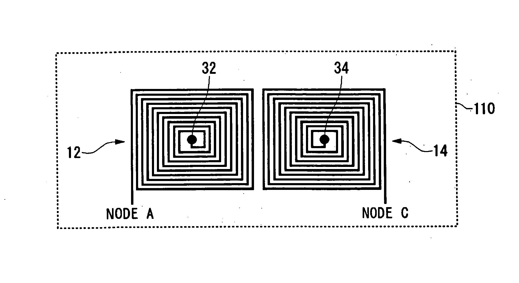
[0057]FIG. 1 is a circuit diagram of an oscillation circuit of an FM tuner according to a first embodiment. An oscillation circuit 10 is provided with a first MOS transistor 20 and a second transistor MOS 22 for high-frequency oscillation. The circuit is also provided with a first inductor 12 and a first variable capacitor 16, a second inductor 14 and a second variable capacitor 18 constituting LC resonance circuits. An LC circuit including the first inductor 12 and the first variable capacitor 16 and an LC circuit including the second inductor 14 and the second variable capacitor 18 are connected in series via a bridge 30. By controlling a voltage applied at a control voltage input terminal 4, the capacitance of the first variable capacitor 16 and the second variable capacitor 18 is changed. This ensures that the oscillation frequency output from an output terminal 6 and an output terminal 8 is variable. Node connected to the output terminal 6 will be referred to ...

second embodiment

(Second Embodiment)

[0085]FIG. 13 is a sectional view showing the structure of a package IC (circuit apparatus) 1A according to a second embodiment. A difference from the first embodiment is that a meander coil pattern instead of a spiral coil pattern is used and the bridge is not exposed in the second wiring layer. The other aspects of the second embodiment are the same as the corresponding aspects of the first embodiment. The second wiring layer may be referred to as a first conductive layer.

[0086] The package IC (circuit apparatus) 1A according to the second embodiment is formed such that the sealing resin 62, the IC chip 60, the die-attach sheet 64, the coating layer (protective layer) 112, a wiring layer 110A, the dielectric layer 115, a first conductive layer 120A and the coating layer 118 are built one on top of another in the stated order. In the first wiring layer 110A, a third inductor 12A of a meandering configuration is formed.

[0087] The outer edge of the IC chip 60 is ...

third embodiment

(Third Embodiment)

[0090]FIGS. 15 and 16 are sectional views showing the structure of a package IC according to a third embodiment. The cross section of FIG. 15 corresponds to the A-A section of the structure of FIG. 3 and the cross section of FIG. 16 corresponds to the B-B section of the structure of FIG. 3. A difference from the first embodiment is that the IC chip 60 is formed of an IC chip 60B and an IC chip 60A located inside the outer edge of the IC chip 60B. The other aspects of the second embodiment are the same as the corresponding aspects of the first embodiment.

[0091] A package IC (circuit apparatus) 1B according to the third embodiment is formed such that the sealing resin 62, the IC chip 60A, the die-attach sheet 64A, the IC chip 60B, the die-attach sheet 64B, the coating layer (protective layer) 112, the first wiring layer 110, the dielectric layer 115, the first conductive layer 120 and the coating layer 118 are built one on top of another in the stated order. A non-c...


PUM


Abstract

A first wiring layer in a circuit substrate structure is provided with a first inductor and a second inductor. A dielectric layer is provided with a first via and a second via electrically connected to the first inductor and the second inductor, respectively. A second wiring layer is provided with: abridge electrically connecting the first via and the second via; and a conductive pattern provided around the bridge, the outer edge of the conductive pattern being located outside the outer edge of the first wiring pattern and the second wiring pattern in the first wiring layer. The bridge functions as a coplanar line and suppresses generation of electromagnetic field.

Description

BACKGROUND OF THE INVENTION [0001] 1. Field of the Invention [0002] The present invention generally relates to a circuit substrate structure on which to mount IC chips and the like and, more particularly, to a circuit substrate structure having multiple wiring layers. [0003] The present invention also relates to a circuit apparatus in which IC chips (circuit elements) and the like are mounted on a circuit substrate structure provided with multiple wiring layers. [0004] 2. Description of the Related Art [0005] It has become common to provide a cell phone with a variety of additional features other than communication functions. A multi-featured cell phone is valued highly in the market and can establish itself as a highly popular model. Particularly in recent years, cell phones with a built-in FM tuner for receiving radio broadcast are gaining popularity. Manufacturers are making efforts to reduce the size of an FM tuner. [0006] An FM tuner requires two spiral coil patterns in an osci...

Claims


Application Information

Patent Timeline
Patent Type & Authority Applications(United States)
IPC IPC(8): H01L29/00
CPCH01F17/0006H01L2924/1305H01L23/49838H01L23/645H01L25/0657H01L2224/32145H01L2924/3011H05K1/0218H05K1/165H05K3/4685H05K2201/0715H01L2225/06568H01L2924/13091H01L23/49822H01L2924/00
Inventor IMAOKA, TOSHIKAZUSAWAI, TETSUROSAITA, ATSUSHIYAMAGUCHI, TAKESHITSUBONOYA, MAKOTOKUROKAWA, KAZUNARI
Owner SANYO ELECTRIC CO LTD
Why Eureka
Try Eureka