Organic electroluminescent device
- Summary
- Abstract
- Description
- Claims
- Application Information
AI Technical Summary
Benefits of technology
Problems solved by technology
Method used
Image
Examples
first embodiment
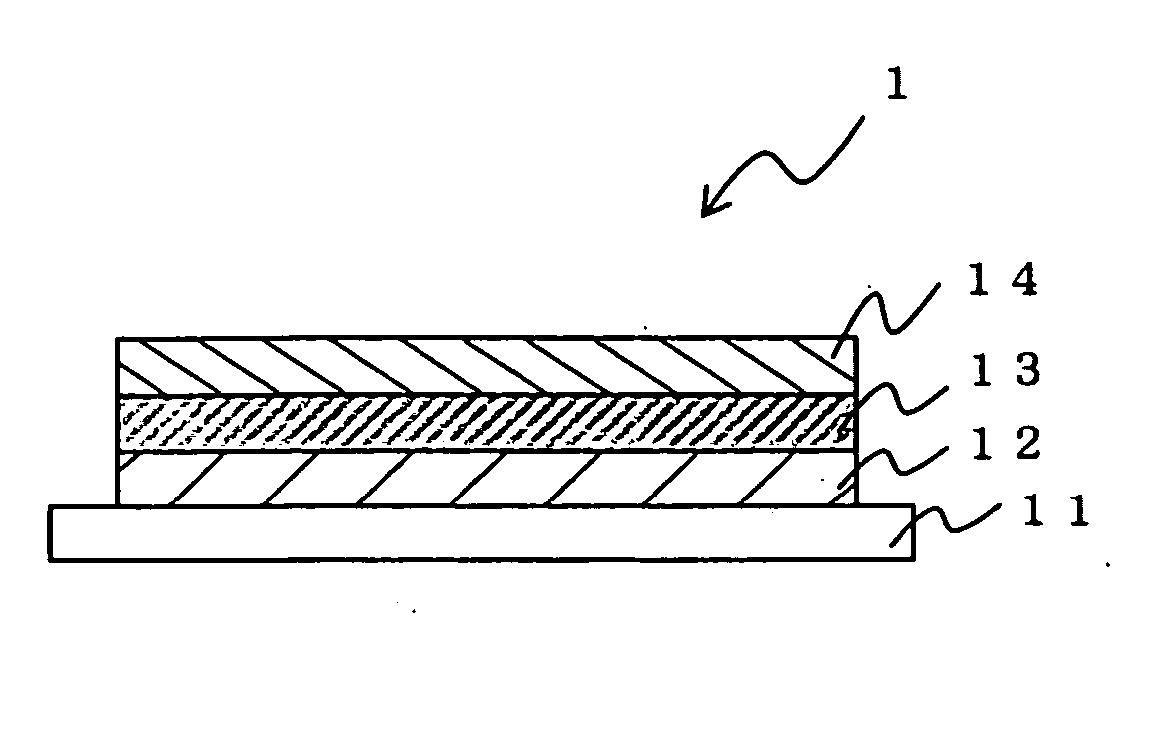
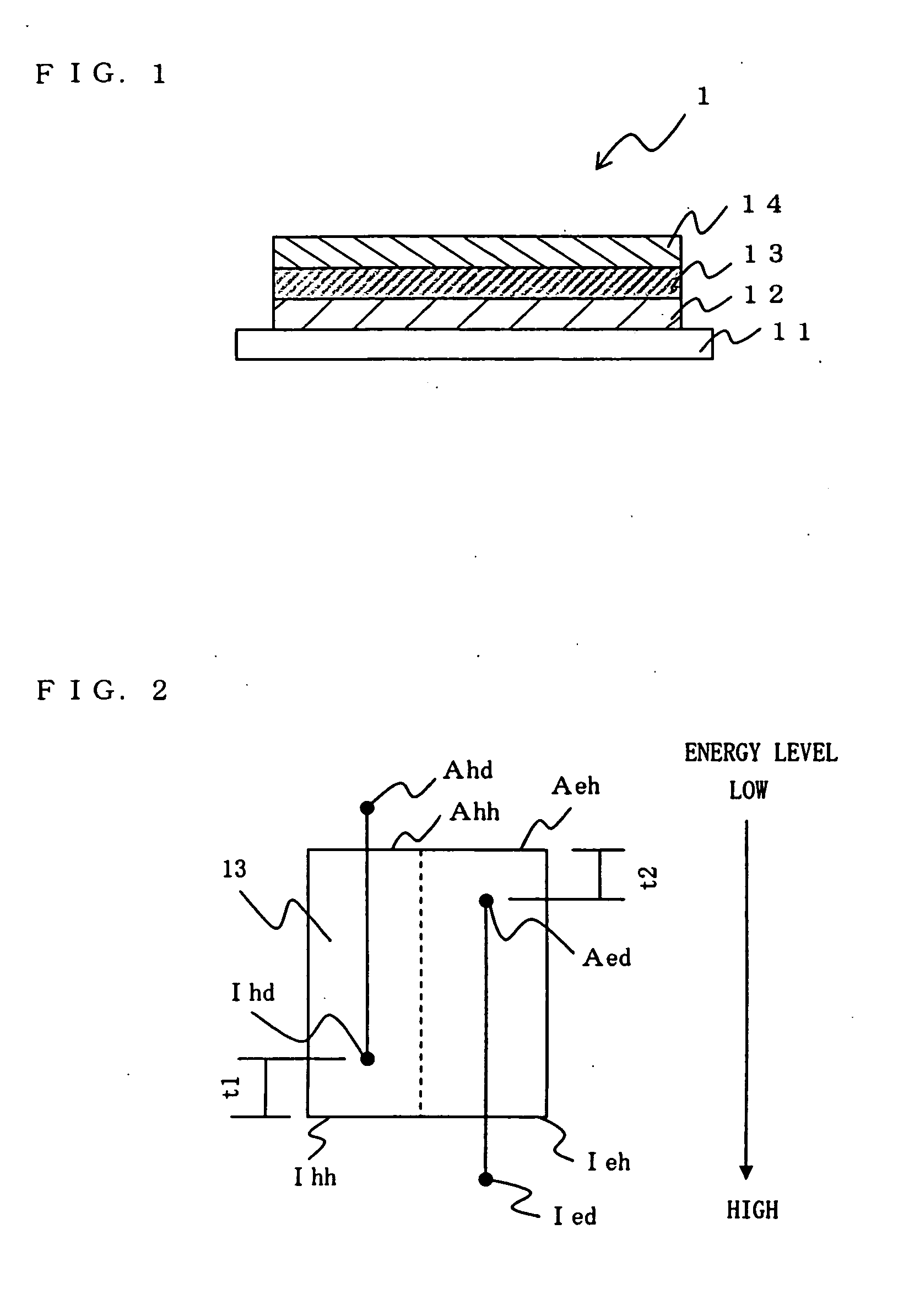
[0020]FIG. 1 is a schematic sectional view of an organic electroluminescent device which is a first embodiment of the invention.
[0021] The organic electroluminescent device 1 has a structure in which an anode 12, an organic emitting layer 13, and a cathode 14 are stacked, in this order, on a substrate 11. In this device, a voltage is applied thereto across the anode 12 and the cathode 14, whereby holes and electrons are injected from the anode 12 and the cathode 14, respectively, to the organic emitting layer 13. These are recombined in the organic emitting layer 13 to emit light.
[0022] In the embodiment, the organic emitting layer 13 is composed of a hole trapping dopant, an electron trapping dopant, a host material containing the hole trapping dopant, and a host material containing the electron trapping dopant.
[0023]FIG. 2 is an energy diagram of the organic electroluminescent device of the embodiment.
[0024] In this energy diagram are shown energy levels (ionization potentials...
second embodiment
[0035] In the organic electroluminescent device of the invention, its organic emitting layer may have a stack structure.
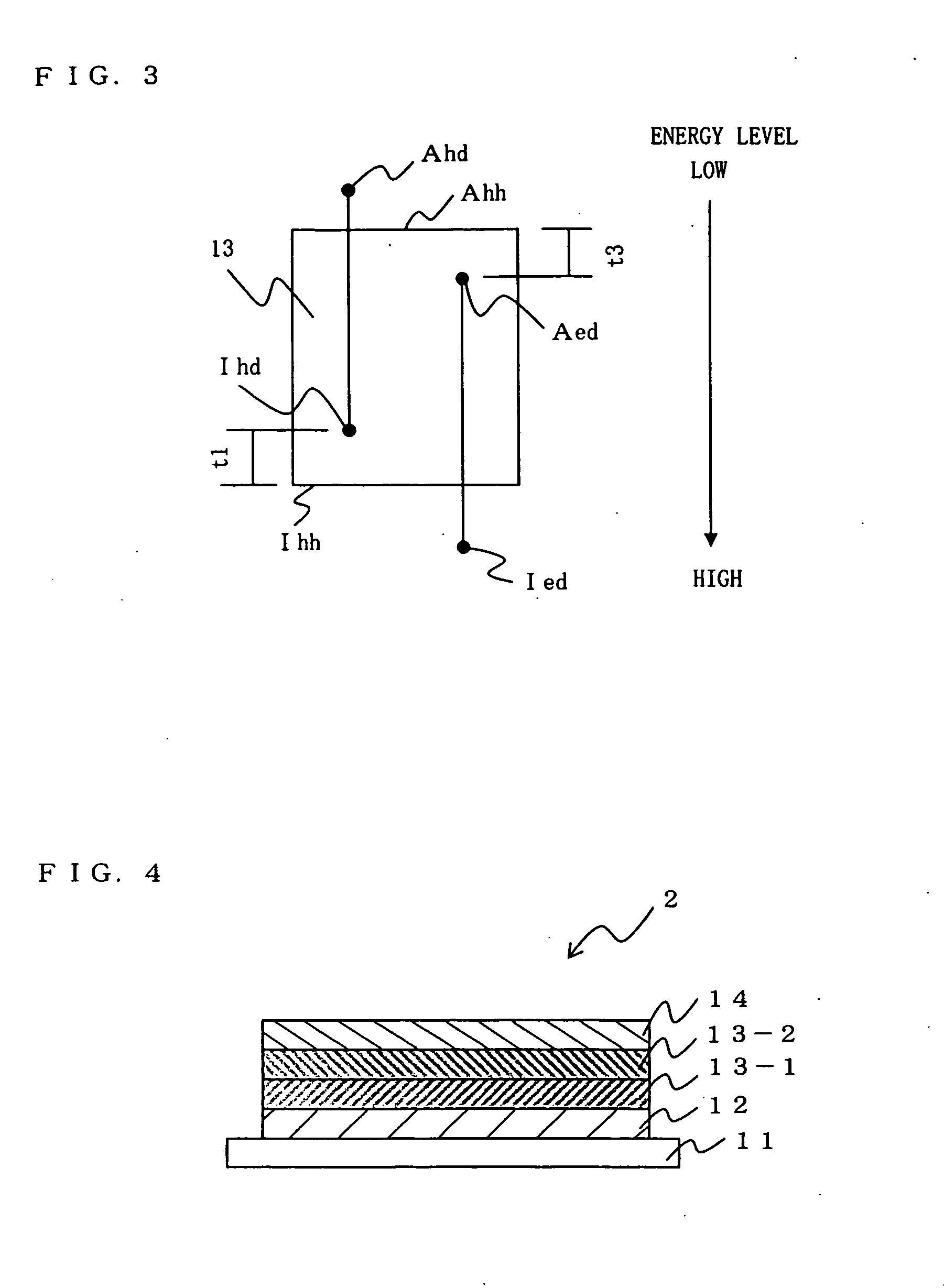
[0036]FIG. 4 is a schematic sectional view of an organic electroluminescent device which is a second embodiment of the invention.
[0037] The organic electroluminescent device 2 has a structure wherein an anode 12, a first organic emitting layer 13-1, a second organic emitting layer 13-2 and a cathode 14 are stacked, in this order, on a substrate 11. When a voltage is applied to this device across the anode 12 and the cathode 14, holes and electrons are injected from the anode 12 and the cathode 14, respectively, to the first organic emitting layer 13-1 and the second organic emitting layer 13-2 so that these are recombined in the first and second organic emitting layers to emit light.
[0038] In the embodiment, the first organic emitting layer 13-1 is made of a first host material and a hole trapping dopant, and the second organic emitting layer 13-2 is made of a s...
example 1
[0171] A glass substrate, 25 mm×75 mm×1.1 mm thick, having an ITO transparent electrode (manufactured by Geomatics Co.) was subjected to ultrasonic cleaning in isopropyl alcohol for 5 minutes followed by UV ozone cleaning for 30 minutes.
[0172] The cleaned glass substrate having transparent electrode lines was set up on a substrate holder in a vacuum deposition device. First, an N,N′-bis(N,N′-diphenyl-4-aminophenyl)-N,N-diphenyl-4,4′-diamino-1,1′-biphenyl film (abbreviated to “TPD 232 film” hereinafter) was formed in a thickness of 60 nm on the surface on which the transparent electrode lines were formed, so as to cover the transparent electrode. This TPD 232 film functioned as a hole-injecting layer.
[0173] After the formation of the TPD 232 film, a 20 nm thick N,N,N′,N′-tetra(4-biphenyl)-diaminobiphenylene layer (abbreviated to “TBDB layer” hereinafter) was formed on the TPD 232 film. This film functioned as a hole-transporting layer.
[0174] Furthermore, a 20 nm thick compound (H1...
PUM
 Abstract
Description
Claims
Application Information
 - R&D
- Intellectual Property
- Life Sciences
- Materials
- Tech Scout
- Unparalleled Data Quality
- Higher Quality Content
- 60% Fewer Hallucinations
Browse by: Latest US Patents, China's latest patents, Technical Efficacy Thesaurus, Application Domain, Technology Topic, Popular Technical Reports.
© 2025 PatSnap. All rights reserved.Legal|Privacy policy|Modern Slavery Act Transparency Statement|Sitemap|About US| Contact US: help@patsnap.com


