
Lattice-mismatched semiconductor structures employing seed layers and related fabrication methods

Inactive Publication Date: 2006-06-22
AMBERWAVE SYST
View PDF5 Cites 115 Cited by
  • Summary
  • Abstract
  • Description
  • Claims
  • Application Information

AI Technical Summary

Benefits of technology

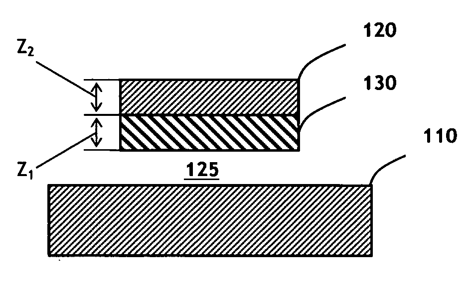
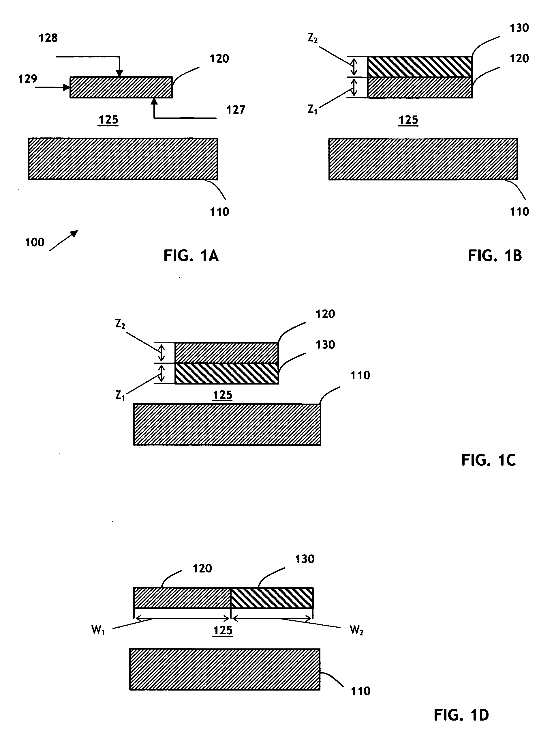
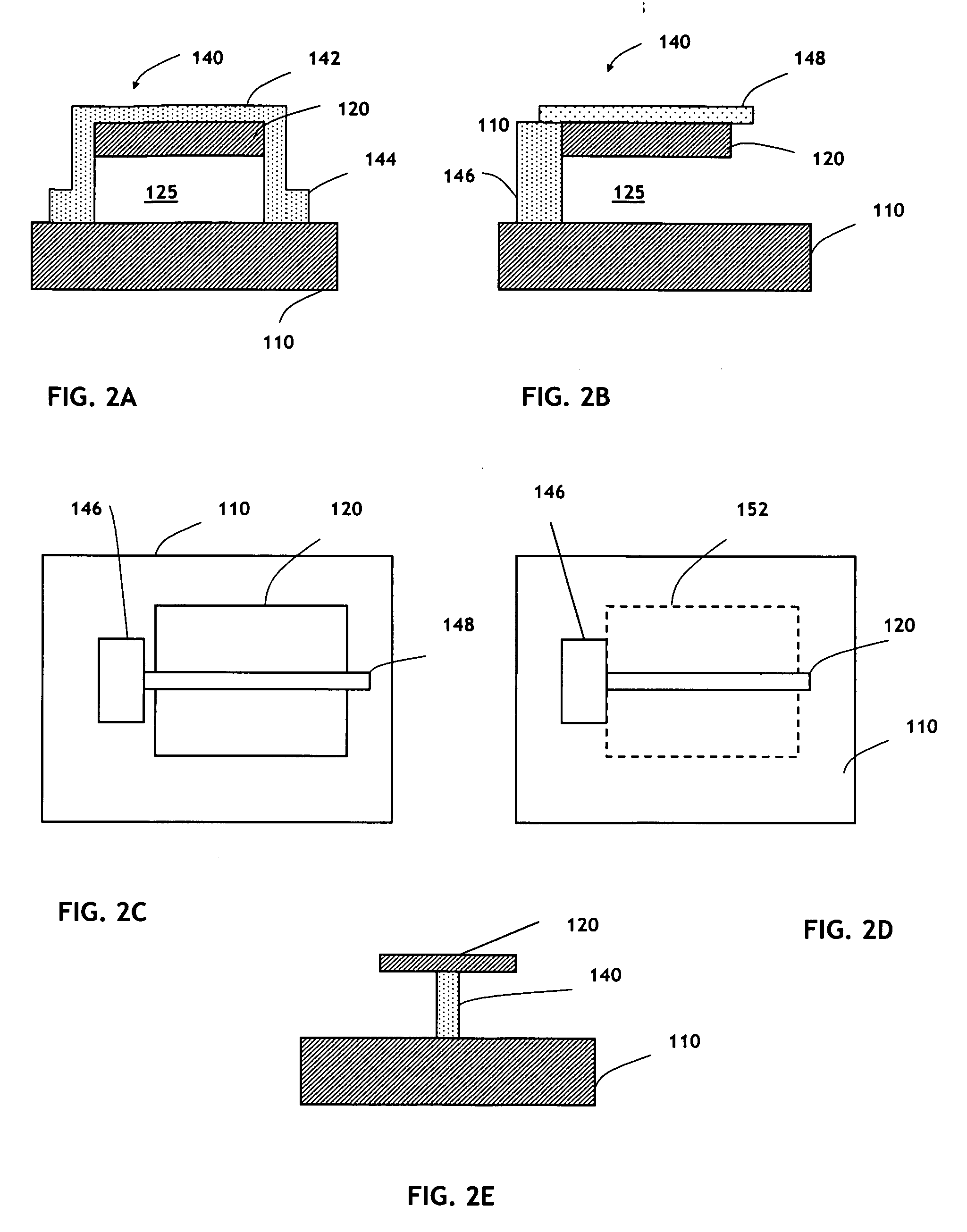
[0013] Accordingly, it is an object of the present invention to provide semiconductor heterostructures with significantly minimized defects, and methods for fabrication of such heterostructures, that address the limitations of known techniques. In its various embodiments, the present invention employs substrate-isolated seed regions for facilitating elastic lattice conformation between the lattice-mismatched materials. Also, relative thicknesses of the materials can be selected to introduce desirable strain distribution within the heterostructure for improved functionality and performance. Further, in certain aspects of the invention, direction and / or type of the strain induced within the heterostructure is controlled. As a result, the invention contemplates fabrication of a variety of semiconductor devices based on monolithic lattice-mismatched heterostructures long sought in the art but heretofore impractical due to dislocation defects.

Problems solved by technology

The increasing operating speeds and computing power of microelectronic devices have recently given rise to the need for an increase in the complexity and functionality of the semiconductor structures from which that these devices are fabricated.
Specifically, a negligible level of dislocation defects is important in a wide variety of semiconductor devices and processes, because dislocation defects partition an otherwise monolithic crystal structure and introduce unwanted and abrupt changes in electrical and optical properties, which, in turn, results in poor material quality and limited performance.
In addition, the threading dislocation segments can degrade physical properties of the device material and can lead to premature device failure.
As mentioned above, dislocation defects typically arise in efforts to epitaxially grow one kind of crystalline material on a substrate of a different kind of material—often referred to as “heterostructure”—due to different crystalline lattice sizes of the two materials.
This lattice mismatch between the starting substrate and subsequent layer(s) creates stress during material deposition that generates dislocation defects in the semiconductor structure.
In addition, dislocation defects can arise in the epitaxial growth of the same material as the underlying substrate where the substrate itself contains dislocations.
Such dislocations in the active regions of semiconductor devices such as diodes, lasers and transistors, may significantly degrade performance.
To minimize formation of dislocations and associated performance issues, many semiconductor heterostructure devices known in the art have been limited to semiconductor layers that have very closely—e.g. within 0.1%—lattice-matched crystal structures.
While lattice matching and near matching eliminate dislocations in a number of structures, there are relatively few lattice-matched systems with large energy band offsets, limiting the design options for new devices.
However, despite the widely recognized potential advantages of such combined structures and substantial efforts to develop them, their practical utility has been limited by high defect densities in gallium arsenide layers grown on silicon substrates.
Due to the limited availability and high cost of large size Ge or III-V wafers, however, the approach may not be practical.
One important limitation of epitaxial necking, however, is the size of the area to which it applies.
Because the seed regions are either part of or connected to the surface of the substrate, the bulky substrate limits the ability of these seed regions to adjust their lattice in order to accommodate the epitaxial growth of the lattice-mismatched material thereover.
Thus, these structures are prone to formation of dislocation defects.

Method used


Image

  • Lattice-mismatched semiconductor structures employing seed layers and related fabrication methods
  • Lattice-mismatched semiconductor structures employing seed layers and related fabrication methods
  • Lattice-mismatched semiconductor structures employing seed layers and related fabrication methods

Examples


Embodiment Construction

[0038] The present invention generally focuses on fabrication of lattice-mismatched semiconductor heterostructures with significantly minimized dislocation defects, as well as on fabrication of various semiconductor devices based on such heterostructures. Also, in certain aspects of the invention, direction, degree, and / or type of the strain induced within the heterostructure is controlled for improved manufacturability, functionality, and performance of the semiconductor devices based thereon. In contrast with the prior art approaches of minimizing dislocation defects, in its various embodiments, the present invention addresses the limitations of known techniques, by utilizing substrate-isolated regions for facilitating elastic lattice conformation between the lattice-mismatched materials.

[0039] As mentioned above, many embodiments of the claimed invention employ semiconductor heterostructures, i.e., structures including two or more layers of semiconductor materials with different...


PUM


Abstract

Fabrication of monolithic semiconductor heterostructures and semiconductor devices based thereon employs isolated seed regions for facilitating elastic lattice conformation between the lattice-mismatched materials. Relative thicknesses of the materials are selected to introduce desirable strain distribution within the heterostructure for improved functionality and performance.

Description

CROSS-REFERENCE TO RELATED APPLICATIONS [0001] This application claims priority to and the benefit of U.S. Provisional Application Ser. No. 60 / 681,940 filed May 17, 2005, and U.S. Provisional Application Ser. No. 60 / 637,132 filed Dec. 18, 2004. The entire disclosures of both of these applications are incorporated herein by reference.FIELD OF THE INVENTION [0002] This invention relates generally to lattice-mismatched semiconductor heterostructures and, more specifically, to integration of dissimilar semiconductor materials employing isolated seed layers. BACKGROUND OF THE INVENTION [0003] The increasing operating speeds and computing power of microelectronic devices have recently given rise to the need for an increase in the complexity and functionality of the semiconductor structures from which that these devices are fabricated. Heterointegration of dissimilar semiconductor materials, for example, III-V materials, such as gallium arsenide, gallium nitride, indium aluminum arsenide, ...

Claims


Application Information

Patent Timeline
IPC IPC(8): H01L31/109
CPCH01L29/66795H01L29/785H01L29/78687
Inventor CHENG, ZHIYUAN
Owner AMBERWAVE SYST
Learn More