Method of forming a polysilicon resistor

a polysilicon resistor and polysilicon technology, applied in resistors, electrical equipment, semiconductor devices, etc., can solve the problems of increasing complexity of circuit designs applying poysilicon resistors to replace load resistors, and achieve the effects of enhancing device integration, high resistance, and reducing the cross section area of polysilicon resistors

Inactive Publication Date: 2006-06-08
UNITED MICROELECTRONICS CORP
View PDF18 Cites 6 Cited by
  • Summary
  • Abstract
  • Description
  • Claims
  • Application Information

AI Technical Summary

Benefits of technology

[0011] It is an advantage of the present invention that the first type dopants and the second type dopants are used to adjust the resistance of the portions of the polysilicon layer within the high resistance region. Being controlled by the dosage adjustment of the first type dopants and the second type dopants, a uniform and stable value of high resistance is therefore obtained to satisfy the circuit designs. In this case, a cross section area of the polysilicon resistor can also be reduced to enhance the device integration.
[0012] These and other objectives of the present invention will no doubt become obvious to those of ordinary skill in the art after reading the following detailed description of the preferred embodiment that is illustrated in the various figures and drawings.

Problems solved by technology

With the development of the various electronic products, circuit designs applying poysilicon resistors to replace load resistors become more and more complicated.

Method used


Image

  • Method of forming a polysilicon resistor
  • Method of forming a polysilicon resistor
  • Method of forming a polysilicon resistor

Examples


Embodiment Construction

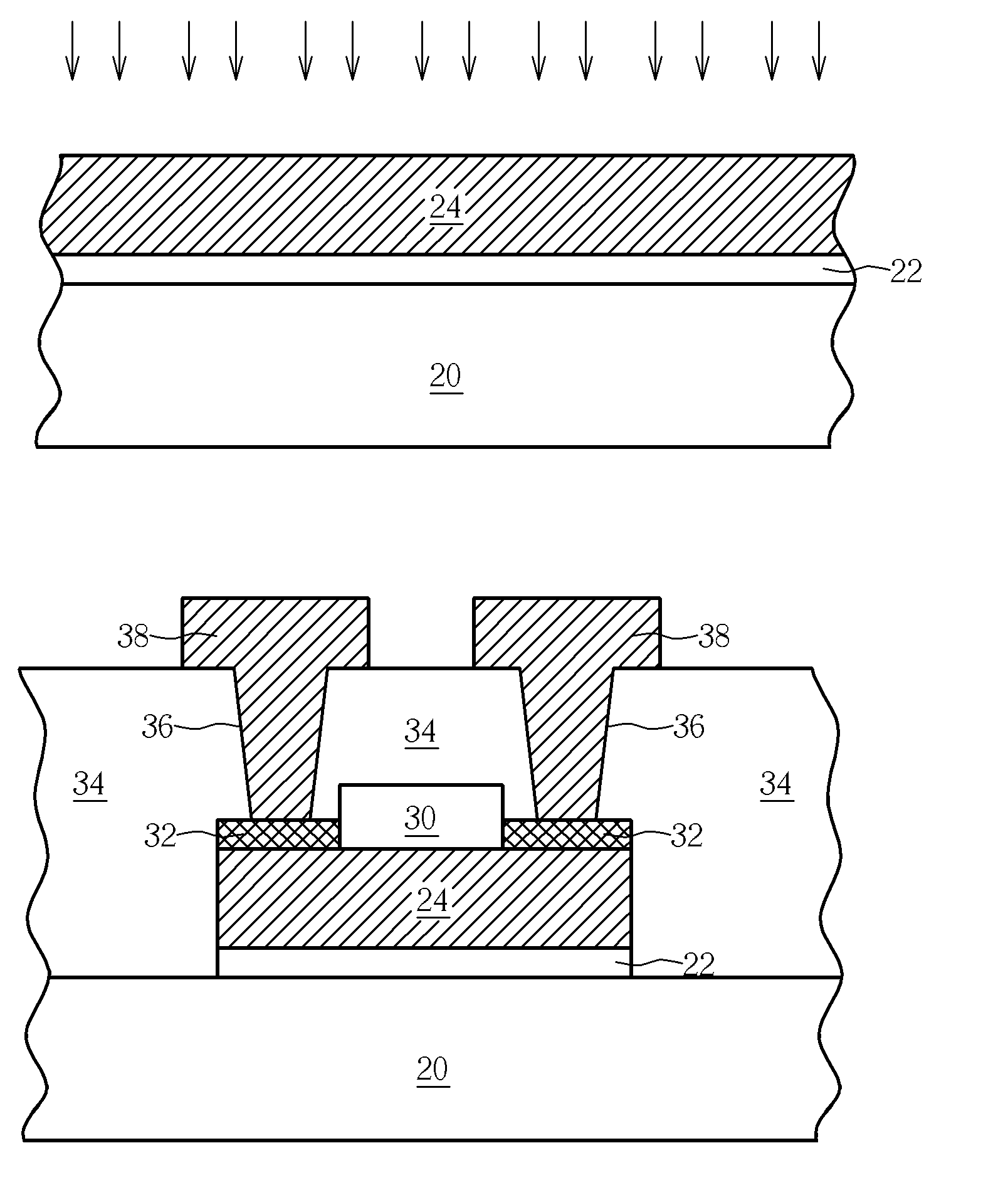
[0015] Referring to FIGS. 4-9, FIGS. 4-9 are schematic diagrams of a method of forming a polysilicon resistor according to the present invention. As shown in FIG. 4, a dielectric layer 22 and a polysilicon layer 24 are formed on a substrate 20, respectively. Following that, as shown in FIG. 5, an ion implantation process is performed using both of N-type dopants and P-type dopants to dope the polysilicon layer 24, thus adjusting the resistance of the polysilicon layer 24. In a better embodiment of the present invention, a dosage of the N-type dopants and a dosage of the P-type dopants have the same order of magnitude. For example, the N-type dopants can be As− ions with a dosage of approximate 3E15, and the P-type dopants can be BF2+ ions with a dosage of approximate 1.5E15. However, the present invention is not limited, other N-type dopants (such as P or Sb) and P-type dopants (such as Ge or B) having the same order of magnitude can also be applied in the present invention to adjus...


PUM


Abstract

A method of forming a polysilicon resistor includes: providing a substrate, the substrate comprising a dielectric layer; forming a polysilicon layer on the dielectric layer; doping the entire polysilicon layer evenly with first type dopants; doping said polysilicon layer containing the first type dopants with second type dopants; defining a polysilicon resistor pattern on the polysilicon layer and removing the polysilicon layer and the dielectric layer outside the polysilicon resistor pattern down to the surface of the substrate, the remainder of the polysilicon layer comprising at least a high resistance region and a low resistance region; and forming a salicide layer on the remainder of the polysilicon layer within the low resistance region.

Description

CROSS REFERENCE TO RELATED APPLICATIONS [0001] This is a continuation application of U.S. application Ser. No. 10 / 711,376, filed Sep. 15, 2004, which is hereby incorporated by reference in its entirety.BACKGROUND OF THE INVENTION [0002] 1. Field of the Invention [0003] The present invention relates to a method of forming a polysilicon resistor, and more particularly, to a method of forming a polysilicon resistor capable of providing a stable value of high resistance. [0004] 2. Description of the Prior Art [0005] In a semiconductor process, polysilicon is often positioned to function as resistors capable of providing high resistance. These resistors can be used in place of load transistors. When load transistors of a static random access memory (SRAM) is replaced by polysilicon resistors, the number of transistors in the SRAM can be reduced and thus saves cost and enhance the integration of the SRAM. [0006] Referring to FIGS. 1-3, FIGS. 1-3 are schematic diagrams of a method of formi...

Claims


Application Information

Patent Timeline
Patent Type & Authority Applications(United States)
IPC IPC(8): H01L21/20
CPCH01L27/0802H01L28/20
Inventor CHEN, CHENG-HSIUNG
Owner UNITED MICROELECTRONICS CORP
Why Eureka
Try Eureka