
Non-volatile semiconductor memory device with alternative metal gate material

a metal gate material and semiconductor technology, applied in semiconductor devices, instruments, electrical appliances, etc., can solve the problems of insufficient or sufficiently fast drop off of the threshold voltage vsub>th /sub> in known sonos devices, poor erase efficiency,

Active Publication Date: 2006-06-08
SAMSUNG ELECTRONICS CO LTD
View PDF5 Cites 112 Cited by
  • Summary
  • Abstract
  • Description
  • Claims
  • Application Information

AI Technical Summary

Benefits of technology

[0030]FIG. 8 illustrates the band gap versus dielectric constant for various oxides.
[0034] FIGS. 12(a), 12(b) and 12(c) illustrate the erasing characteristics −10 volts bias −12 volts bias and −14 volts bias, respectively.
[0035]FIG. 13 illustrates the voltage threshold versus erase time of an O / SiN / H / M charge trapping non-volatile memory device in accordance with an exemplary embodiment of the present invention.

Problems solved by technology

A drawback of these types of memory devices results from a characteristic relatively poor erasing efficiency that prevents them from meeting backwards compatibility requirements of a 10−3 second erasing time at around −3 volts for the threshold voltage Vth (V)).
The known charge trap flash memory devices have this problem by reason of electrons back tunneling through the blocking layer.
Electronic back tunneling causes the erase threshold voltage Vth to not drop off sufficiently or sufficiently quickly in known SONOS devices.
This back tunneling means that electrons are provided to the charge trapping layer from the control gate thereby reducing or slowing the drop in population of electrons, resulting in lengthened erase operation and otherwise lowering the erase efficiency.
That is, the combination of metal and silicon tends to be unstable.
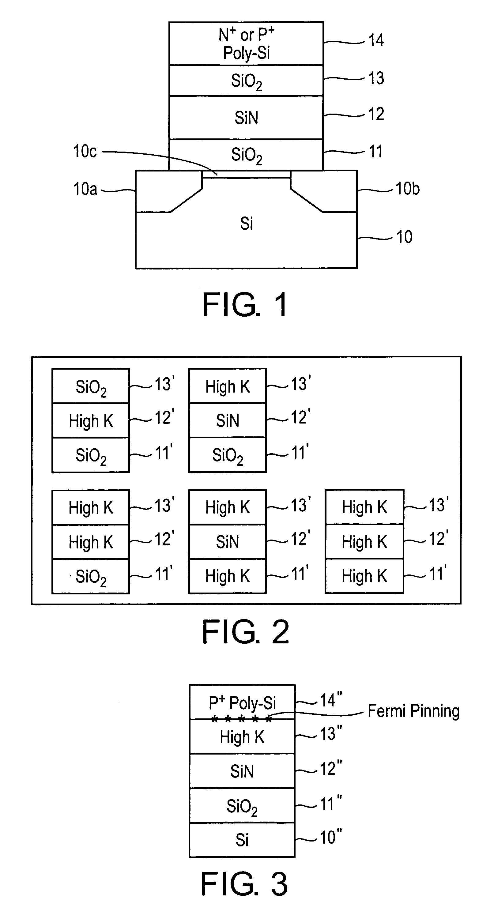
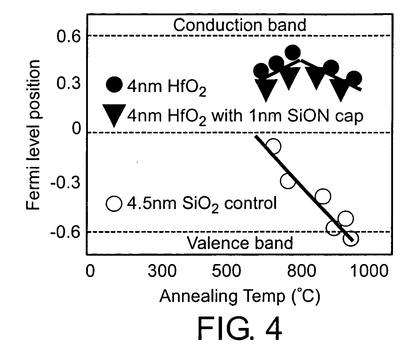
As reported in E. Cartier et al., “Systemic Study of pFET Vt with Hf-Based Gate Stacks with Poly-Si and FUSI Gates,” VLSI 2004-VLSI Technology / Circuits Symposium, IEEE, June, 2004, the perceived problem with this structure is the apparent effect of Fermi level pinning in the HfO2.
Accordingly, materials with high κ are not compatible with a gate that is formed of p+ poly-silicon regardless of the annealing temperature used for the material because of the back tunneling effect.
The back tunneling effect results in relatively poor erasing efficiency.
It thus appears that Fermi level pinning occurs interferes in this structure at least with respect to its usefulness in a charge trapping dielectric non-volatile memory device.

Method used


Image

  • Non-volatile semiconductor memory device with alternative metal gate material
  • Non-volatile semiconductor memory device with alternative metal gate material
  • Non-volatile semiconductor memory device with alternative metal gate material

Examples


Embodiment Construction

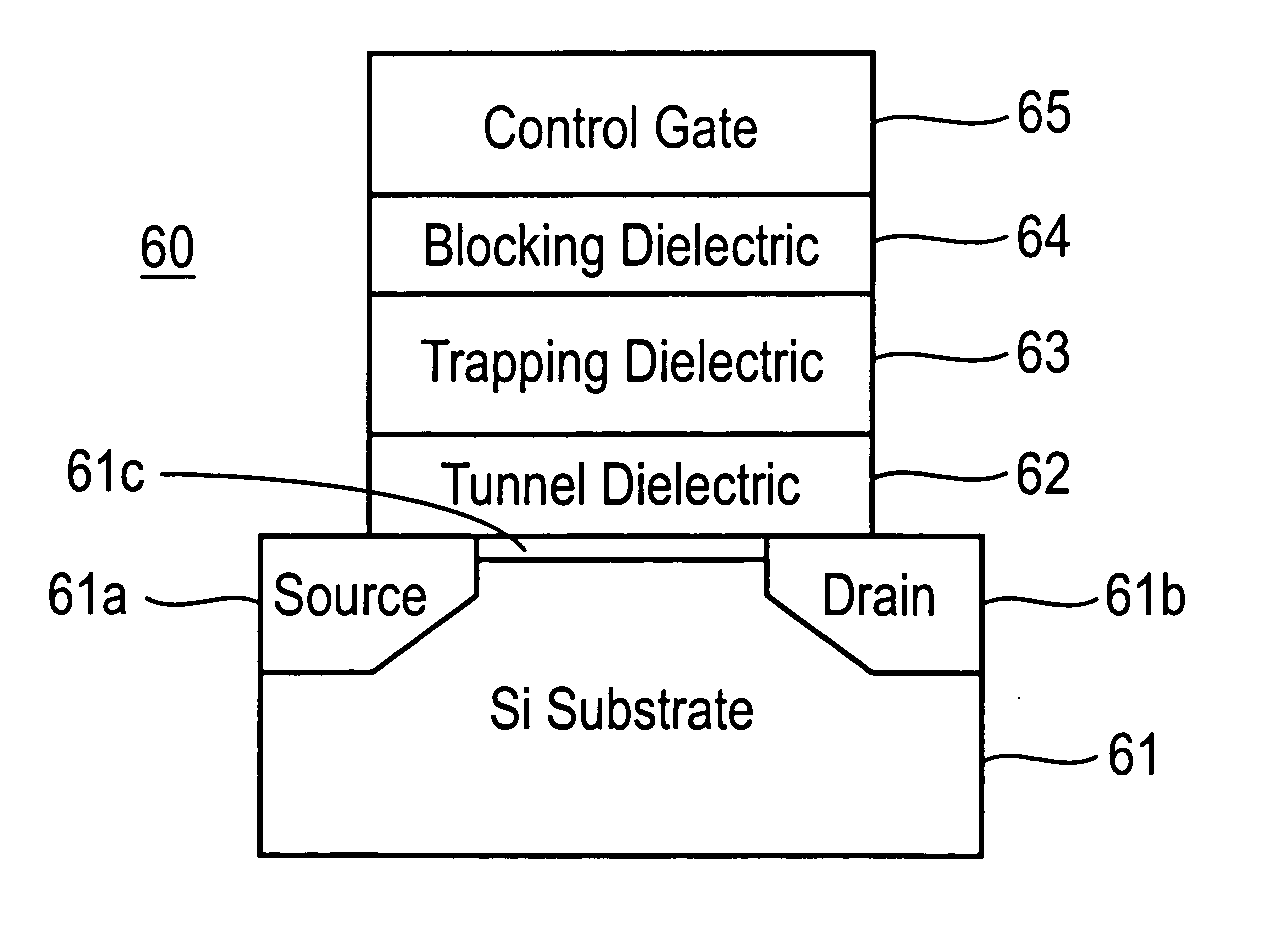
[0036] The present invention will now be described more fully with reference to the accompanying drawings, in which exemplary embodiments of the invention are shown. The invention may, however, be embodied in many different forms and should not be construed as being limited to the embodiments set forth herein; rather, these embodiments are provided so that this disclosure will be thorough and complete, and will fully convey the concept of the invention to those skilled in the art.

[0037]FIG. 5 illustrates a floating gate stack-type non-volatile memory 50, which includes a substrate 51 made of, for example, silicon. Other materials for the substrate 51 can be used, but silicon is currently the most common. In the substrate 51 are formed a source 51a and a drain 51b between which is formed a channel region 51c. It should be noted that, in this instance, the term “substrate” should be interpreted broadly to include wafers or other forms of substrates whether rigid or flexible, and also...


PUM


Abstract

A non-volatile semiconductor memory device comprises a substrate including a source region, a drain region and a channel region provided between the source region and the drain region with a gate stack located above the channel region with a metal gate located above the gate stack. The metal gate is comprised of a metal having a specific metal work function relative to a composition of a layer of the gate stack that causes electrons to travel through the entire thickness of the blocking layer via direct tunneling. The gate stack preferably comprises a multiple layer stack selected from a group of multiple layer stacks consisting of: ONO, ONH, OHH, OHO, HHH, or HNH, where O is an oxide material, N is SiN, and H is a high κ material.

Description

CROSS-REFERENCE TO RELATED PATENT APPLICATION [0001] Priority is claimed to Korean Patent Application No. 10-2004-0080354, filed on Oct. 8, 2004, in the Korean Intellectual Property Office, the disclosure of which is incorporated herein in its entirety by reference. FIELD OF THE INVENTION [0002] The present invention relates to non-volatile semiconductor memory devices including charge trap flash memory and floating gate flash memory devices, as well as to methods of making non-volatile semiconductor memory devices. DESCRIPTION OF RELATED ART [0003] Non-volatile memory devices are electronic memory devices that retain their content when external power is removed. Semiconductor non-volatile memory devices typically include a charge trapping layer in which charges are trapped between a gate and a channel region of a transistor. The trapped charges create a threshold voltage difference in the channel region. The threshold voltage Vth varies depending on whether the non-volatile memory ...

Claims


Application Information

Patent Timeline
IPC IPC(8): H01L29/788
CPCG11C16/0416G11C16/0466H01L21/28273H01L21/28282H01L29/513H01L29/7881H01L29/792H01L29/40114H01L29/40117
Inventor JEON, SANG-HUNHAN, JEONG-HEEKIM, CHUNG-WOO
Owner SAMSUNG ELECTRONICS CO LTD
Learn More