
Multiple bit chalcogenide storage device

a chalcogenide storage device and multi-bit technology, applied in the field of chalcogenide storage devices, can solve the problems of capacitor charge not being permanently stored, data cannot be removed from rom, and can only be read, and the capacitor charge cannot be permanently stored, etc., to achieve the effect of preventing leakage to the substrate on which the dram cell is located or to neighboring devices

Inactive Publication Date: 2006-06-08
OVONYX MEMORY TECH LLC
View PDF3 Cites 18 Cited by
  • Summary
  • Abstract
  • Description
  • Claims
  • Application Information

AI Technical Summary

Benefits of technology

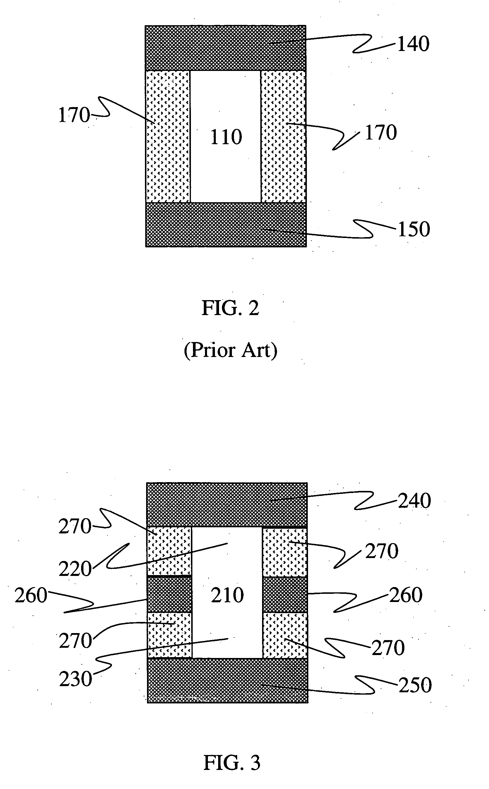
[0015] In one embodiment of the instant invention, selective programming of individual portions of chalcogenide material within a larger volume of chalcogenide material having one or more compositions is provided. In this embodiment, a programming pulse applied between a pair of electrical terminals of a device induces a structural transformation in a portion of chalcogenide material between that pair of electrical terminals without inducing a structural transformation of chalcogenide material in the vicinity of other terminals. In this embodiment, data storage in one portion of a chalcogenide material occurs without disturbing the information content of an adjacent portion of chalcogenide material.

Problems solved by technology

Data is pre-recorded on ROM and once recorded, data cannot be removed from ROM, but rather can only be read.
The capacitor charge is not stored permanently, however, and shows a tendency to leak to the substrate on which the DRAM cell is located or to neighboring devices on a chip.
The refreshing requirement drives up power consumption and underlies the volatile characteristic of DRAM.
SRAM is faster than DRAM, but also more expensive because an SRAM memory cell requires more transistors than DRAM (typically 4-6 transistors as opposed to one for DRAM) and requires more space on a chip.
But given its higher cost, however, it is primarily used in cache memory applications, where high speed is essential.
First, the write time of flash memory is slow (on the order of a microsecond) and limits the range of applications for flash memory.
While suitable for archival storage, flash is unsuitable for use as a working memory because competitive data processing requires fast writing times. Second, the lifetime of flash memory is relatively short as the reliability of data storage in flash memory diminishes after a few hundred thousand write-erase cycles.
Recent advances in conventional flash memory, however, have raised the entry barrier for a replacement flash technology.
As a result, the cost per stored bit of information has dropped considerably in current flash technology and the performance and cost standards for a competing replacement technology have increased commensurately.
At this point in time, it is unknown whether any of the three currently identified replacement flash technologies will prove to be better than the others and whether any of them will perform well enough to displace conventional flash technology.

Method used


Image

  • Multiple bit chalcogenide storage device
  • Multiple bit chalcogenide storage device
  • Multiple bit chalcogenide storage device

Examples


Embodiment Construction

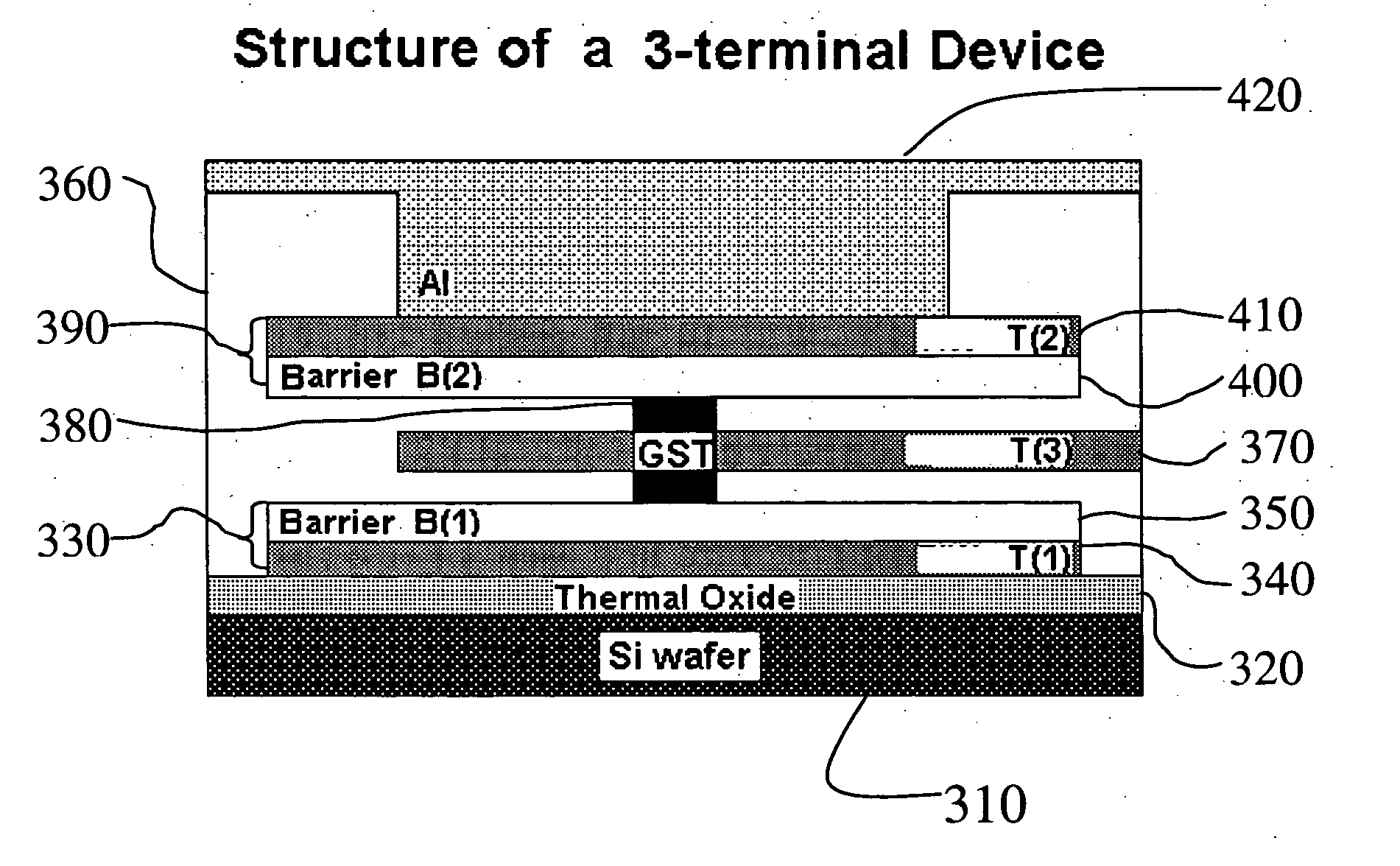
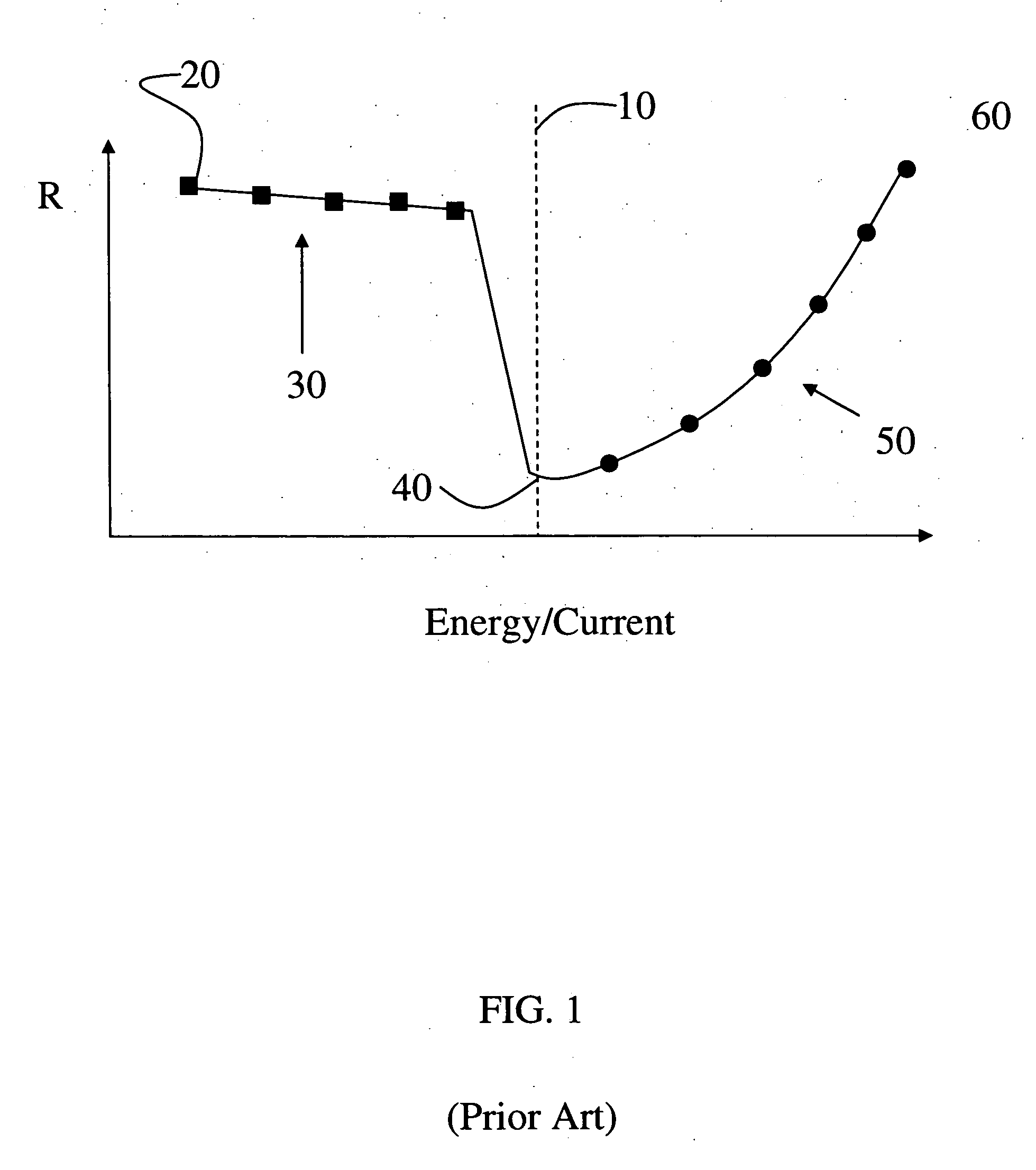
[0026] The instant invention provides a memory cell capable of multibit data storage and a method for programming a memory cell to store two or more bits of information. The memory cell of the instant invention includes a volume of chalcogenide material in electrical communication with three or more electrical terminals where electrical energy provided to the electrical terminals is used to program the chalcogenide material to store data. The chalcogenide material is the data storage medium of the instant memory cell. The chalcogenide material is a phase change material that is capable of reversibly transforming among a plurality of structural states by providing electrical energy in the form of an electrical current or voltage pulse. The different structural states of the phase change material are distinguishable on the basis of a characteristic property such as electrical resistance and each can be uniquely associated with different information states to provide the basis of a dat...


PUM


Abstract

Multi-terminal chalcogenide memory cells having multiple binary or non-binary bit storage capacity and methods of programming same. The memory cells include a pore region containing a chalcogenide material along with three or more electrical terminals in electrical communication therewith. The configuration of terminals delineates spatially distinct regions of chalcogenide material that may be selectively and independently programmed to provide multibit storage. The application of an electrical signal (e.g. electrical current or voltage pulse) between a pair of terminals effects a structural transformation in one of the spatially distinct portions of chalcogenide material. Application of electrical signals to different pairs of terminals within a chalcogenide device effects structural transformations in different portions of the chalcogenide material. The structural states produced by the structural transformations may be used for storage of information values in a binary or non-binary (e.g. multilevel) system. The selection of terminals provides for the selective programming of specific and distinct portions within a continuous volume of chalcogenide material, where each selectively programmed portion provides for the storage of a single binary or non-binary bit. In devices having three or more terminals, two or more selectively programmable portions are present within the volume of chalcogenide material occupying the pore region and multibit storage is accordingly realized. The instant invention further includes methods of programming chalcogenide memory cells having three or more terminals directed at the storage of multiple bits of information in binary or non-binary systems.

Description

CROSS-REFERENCE TO RELATED APPLICATIONS [0001] This application is a division of application Ser. No. 10 / 657,285, filed Sep. 8, 2003, the disclosure of which is herein incorporated by reference.FIELD OF INVENTION [0002] This invention relates to chalcogenide storage devices. More particularly, this invention relates to devices having multiple terminals in electrical communication with a chalcogenide material in which different pairs of terminals are capable of programming different portions of the chalcogenide material. Most particularly, this invention relates to chalcogenide devices that provide a multiple bit data storage capability. BACKGROUND OF THE INVENTION [0003] Computers and consumer electronics are critically dependent on the memories used to store and process information. Various types of memories, including ROM, RAM, DRAM, SRAM and flash, underlie the storage and processing capabilities of computers and consumer electronics. These different forms of memory differ with r...

Claims


Application Information

Patent Timeline
Patent Type & Authority Applications(United States)
IPC IPC(8): H01L47/02H10N80/10G11CG11C11/00G11C11/56G11C16/02G11C27/00G11C29/00H01L31/0328H10N80/00
CPCG11C11/56G11C11/5678G11C13/0004H01L45/144H01L45/1206H01L45/1233H01L45/1246H01L45/06H10N70/253H10N70/828H10N70/231H10N70/8828H10N70/826H10N70/8825
Inventor OVSHINSKY, STANFORD R.
Owner OVONYX MEMORY TECH LLC
Learn More