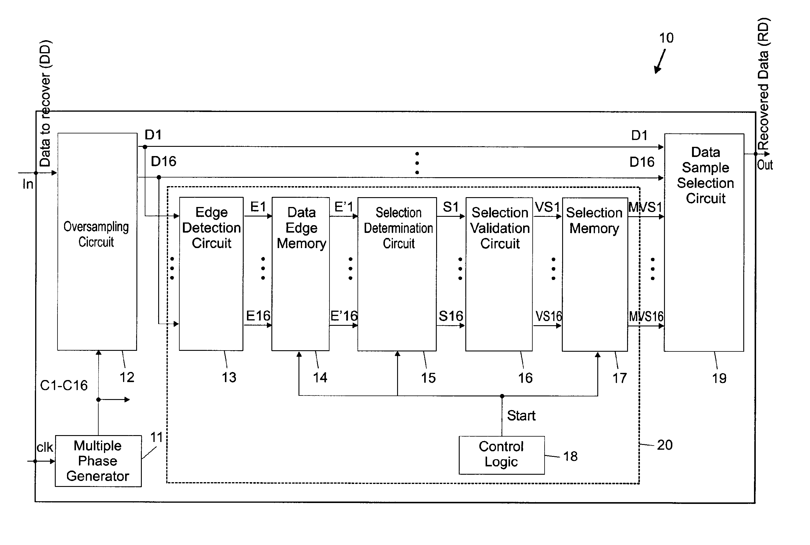
Improvements to data recovery circuits using oversampling for best data sample selection
a data recovery circuit and data sample technology, applied in the field of high-speed serial communication/data transfer, can solve the problems of significant reduction of the useful sampling window, negative impact on the sampling window width and thus on the targeted circuit accuracy, and the data recovery circuit built for a given communication data protocol is generally not suitable for recovering data
- Summary
- Abstract
- Description
- Claims
- Application Information
AI Technical Summary
Benefits of technology
Problems solved by technology
Method used
Image
Examples
example 1
[0040] Example 1 represents E′ values for single data rate (SDR) data without jitter. The position of the single ‘0’ corresponds to the sample position where a data transition was detected.
1 1 1 1 1 0 1 1 1 1 1 1 1 1 1 1
[0041] Example 2 represents E′ values for single data rate (SDR) data with jitter. The transition position varies in time due to the presence of jitter, so that more than one data transitions are detected.
1 1 1 0 0 0 1 1 1 1 1 1 1 1 1
[0042] The zone filled with ‘0’s corresponds to the grayed zone in the eye diagram of FIG. 1.
[0043] Example 3 represents E′ values for double data rate (DDR) data without jitter. As there are now two bits of data per clock period, two data transition positions were detected.
1 1 1 1 1 0 1 1 1 1 1 1 1 1 0 1 1
example 4
[0044] Example 4 represents E′ values for DDR data with jitter. The presence of jitter on the incoming data stream has the effect of moving the detected data edge randomly around a central position. The effect on the E′ values is to increase the width of the zones with adjacent ‘0’s.
1 1 1 1 0 0 0 1 1 1 1 1 0 0 0 1
[0045] Therefore, the edge information is presented under the form of a bit map. A bit set to ‘0’ indicates that a data edge has been detected at this corresponding sample position during the duration of a previous edge search and a bit set to ‘1’ indicates a sample position where no data edge was seen during the same duration. Assuming a reasonable level of jitter and further assuming the edge information is collected for a long duration compared to the data bit period, then the bit map appears as one zone (SDR) or two zones (DDR) filled with adjacent ‘0’s (corresponding to the zone where data edges were detected) surrounded by adjacent ‘1’s. The last bit map position is...
PUM
 Abstract
Description
Claims
Application Information
 - R&D
- Intellectual Property
- Life Sciences
- Materials
- Tech Scout
- Unparalleled Data Quality
- Higher Quality Content
- 60% Fewer Hallucinations
Browse by: Latest US Patents, China's latest patents, Technical Efficacy Thesaurus, Application Domain, Technology Topic, Popular Technical Reports.
© 2025 PatSnap. All rights reserved.Legal|Privacy policy|Modern Slavery Act Transparency Statement|Sitemap|About US| Contact US: help@patsnap.com


