Light emitting diode component

a technology of light emitting diodes and components, applied in the field of single-chip and multiple-chip light emitting diodes, can solve the problems of low light output intensities low light output intensity of early light emitting diodes, and general inability to compete with incandescent and fluorescent light sources. , to achieve the effect of improving the efficiency of light emitting packages, and improving the efficiency of light emitting

Active Publication Date: 2006-05-11
GENERAL ELECTRIC CO +1
View PDF62 Cites 221 Cited by
  • Summary
  • Abstract
  • Description
  • Claims
  • Application Information

AI Technical Summary

Benefits of technology

[0016] According to another aspect, a method is provided for making a light emitting package. At least one light emitting die is electrically and mechanically connected to a printed circuit board. A light transmissive cover is secured to the printed circuit board. The light transmissive cover covers the at least one light emitting die. The secured light transmissive cover and the printed circuit board cooperatively define an interior volume. An encapsulant is disposed in the interior volume.

Problems solved by technology

One issue with light emitting diode components or packages relates to light output intensity.
Early light emitting diodes had low light output intensities and were generally not competitive with incandescent and fluorescent light sources.
Another issue with light emitting diode components and packages relates to ruggedness.
Commonly used packaging techniques, such as bonding of the dice to lead frames, can produce relatively fragile light emitting packages.
Moreover, light emitting diode components and packages tend to be complex.
Multiple chip packages generally further increase complexity.
Baretz discloses a phosphor contained in an encapsulant disposed inside the housing, The complexity of multiple chip packages such as those of Lowery and Baretz can adversely impact manufacturability, reliability, and manufacturing costs.
Another issue with typical light emitting diode packages and components is operating lifetime.
Performance of packages employing phosphor wavelength conversion of ultraviolet or short-wavelength visible light typically degrades over time due to discoloration or other degradation of the encapsulant or other materials caused by the ultraviolet or short-wavelength visible light irradiation.
Another issue with typical light emitting diode packages is plug-in capability with lighting fixtures.
Such plug-in fixture compatibility is, however, hampered by the typically high voltage and / or high frequency electrical power supplied by such fixtures, which is not conducive to powering low-voltage light emitting diode devices.
Another issue with using light emitting diode packages for illumination is light output quality.
When light emitting diode packages employ several light emitting chips so as to produce high light intensity, a problem arises in that the output consists of several approximate point light sources corresponding to the several chips.
This pixelated spatial distribution of light is problematic for illumination applications.
Spectral light output quality can also be an issue when using light emitting diode packages for white illumination.
Obtaining white light or substantially white light with a desired (usually high) CRI value in a commercially practical manner is difficult.

Method used


Image

  • Light emitting diode component
  • Light emitting diode component
  • Light emitting diode component

Examples


Embodiment Construction

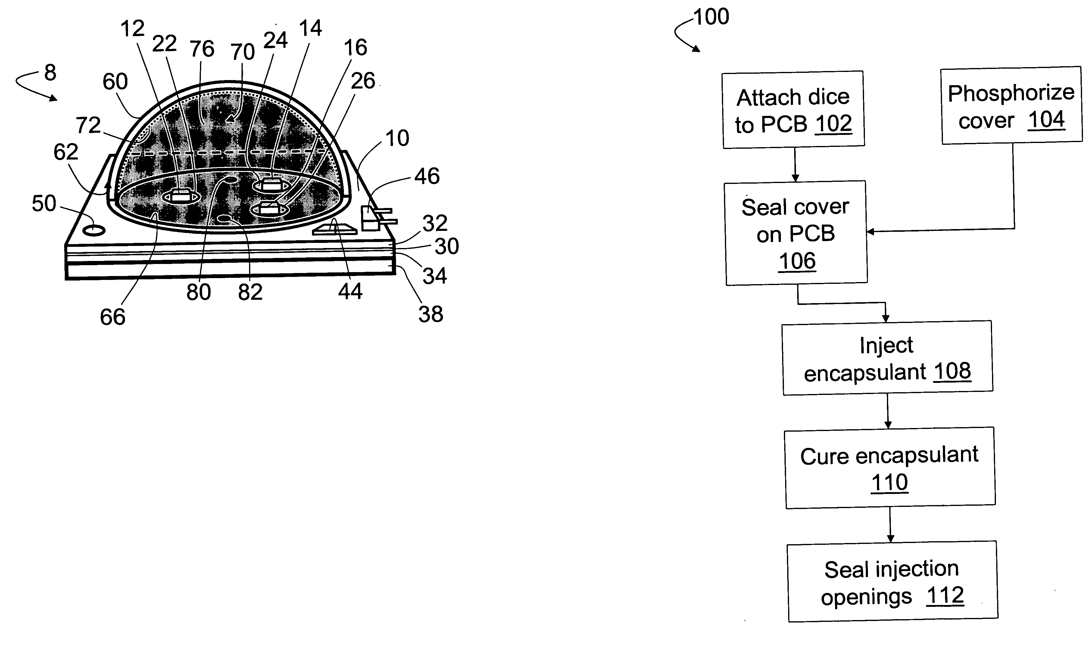
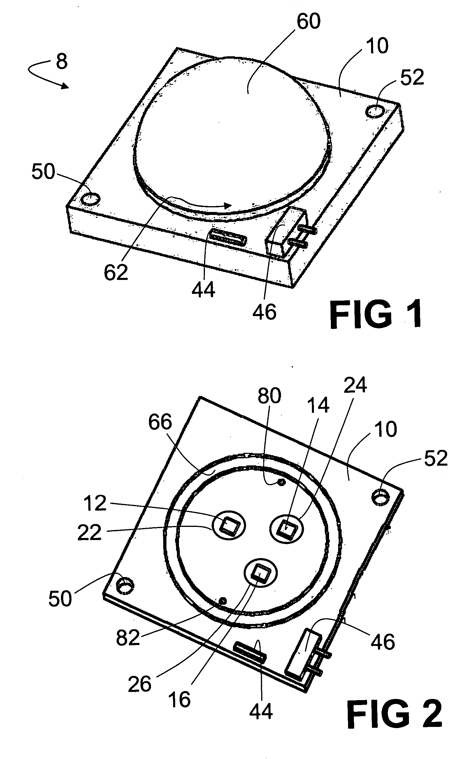
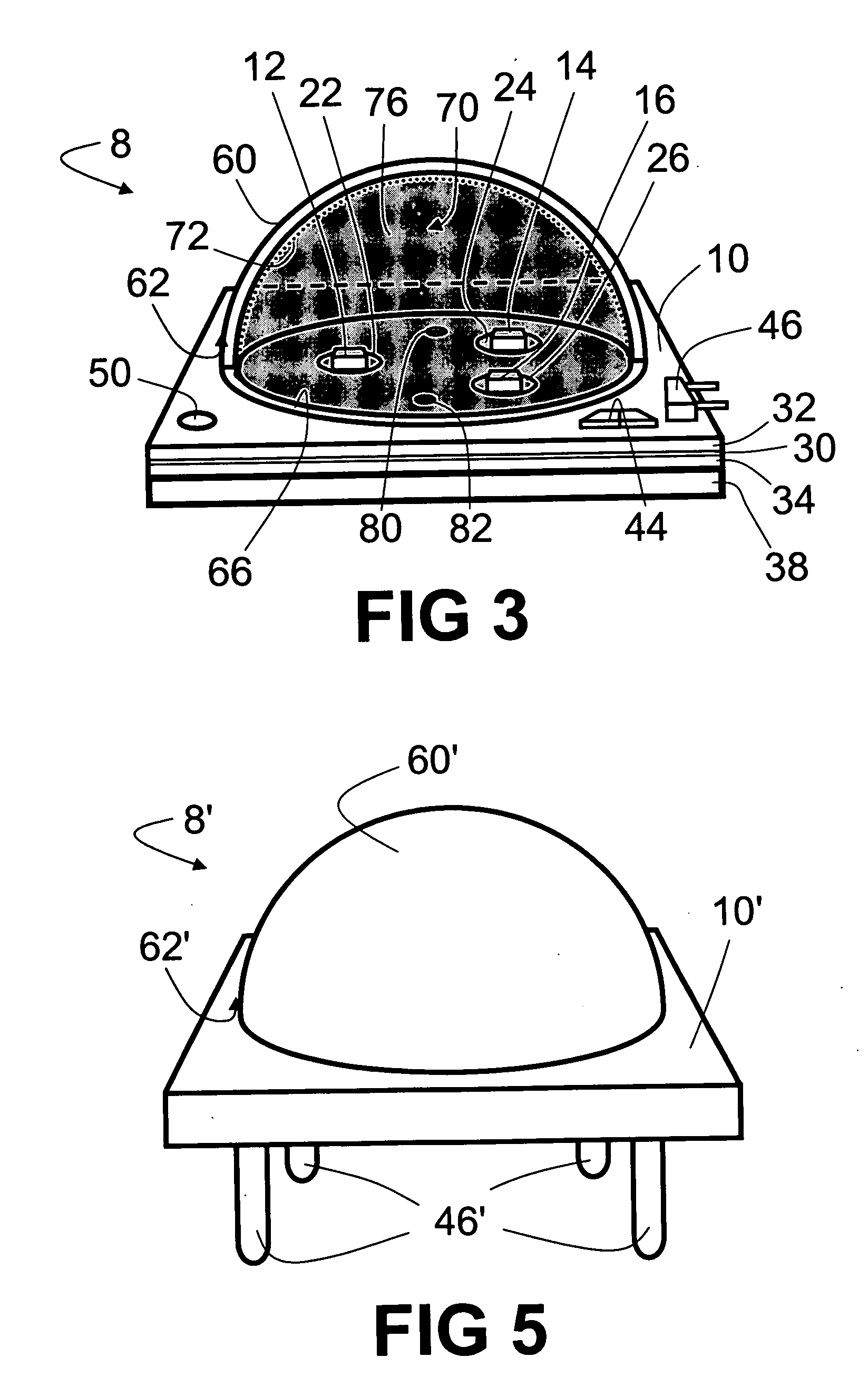
[0039] With reference to FIGS. 1-3, a light emitting package 8 includes a printed circuit board 10 on which one or more light emitting chips or die are disposed. The printed circuit board is preferably substantially thermally conductive. For example, a metal core printed circuit board can be employed. In the illustrated embodiment, three light emitting chips or dice 12, 14, 16 are disposed on the circuit board 10; however, the number of dice can be one die, two dice, or more than three dice. The die or dice can be group III-nitride blue or ultraviolet light emitting diodes, red group III-phosphide or group III-arsenide light emitting diodes, II-VI light emitting diodes, IV-VI light emitting diodes, silicon or silicon-germanium light emitting diodes, or the like. As used herein, the term “ultraviolet” is intended to encompass light emitting diode emission having a peak wavelength less than or about 425 nm. In some contemplated embodiments, the die or dice are edge emitting lasers or ...


PUM


Abstract

In a lighting package, a printed circuit board supports at least one light emitting die. A light transmissive cover is disposed over the at least one light emitting die. A phosphor is disposed on or inside of the light transmissive dome-shaped cover. The phosphor outputs converted light responsive to irradiation by the at least one light emitting die. An encapsulant substantially fills an interior volume defined by the light-transmissive cover and the printed circuit board.

Description

[0001] This application is a continuation-in-part of application Ser. No. 10 / 831,862 filed Apr. 26, 2004 which is a continuation-in-part of International Application number PCT / US2003 / 027363 with an international filing date of Aug. 29, 2003 first published Mar. 11, 2004 as International Publication no. WO 2004 / 021461 A2, which claims the benefit of U.S. Provisional Application Ser. No. 60 / 407,426 filed on Aug. 30, 2002. This application is also a continuation-in-part of application Ser. No. 10 / 909,564 filed Nov. 2, 2004. [0002] This application incorporates by reference the content of application Ser. No. 10 / 831,862, which has published as US 2005-0239227 A1. This application incorporates by reference the content of International Application number PCT / US2003 / 027363. This application incorporates by reference the content of U.S. Provisional Application Ser. No. 60 / 407,426. This application incorporates by reference the content of application Ser. No. 10 / 909,564.BACKGROUND [0003] Th...

Claims


Application Information

Patent Timeline
Patent Type & Authority Applications(United States)
IPC IPC(8): H01L23/02H01L29/06H01L31/0328H01L31/0336H01L31/072H01L31/109F21K99/00
CPCF21K9/00H01L25/0753H01L33/507H01L2224/48091H01L2924/00H01L2924/01322F21V23/00F21K9/68H01L2924/00014
Inventor AANEGOLA, SRINATH K.RADKOV, EMIL V.REGINELLI, JAMESSTADELMAN, LARRY R.MRAKOVICH, MATTHEWSTIMAC, TOMISLAV J.
Owner GENERAL ELECTRIC CO
Why Eureka
Try Eureka