Method for setting erasing pulse and screening erasing defect of nonvolatile memory
- Summary
- Abstract
- Description
- Claims
- Application Information
AI Technical Summary
Benefits of technology
Problems solved by technology
Method used
Image
Examples
Embodiment Construction
[0033] Embodiments of a method for setting erasing pulse and an erasing defect screening method according to the present invention (referred to as a “setting method of the present invention” and a “screening method of the present invention” hereinafter) will be described referring the relevant drawings.
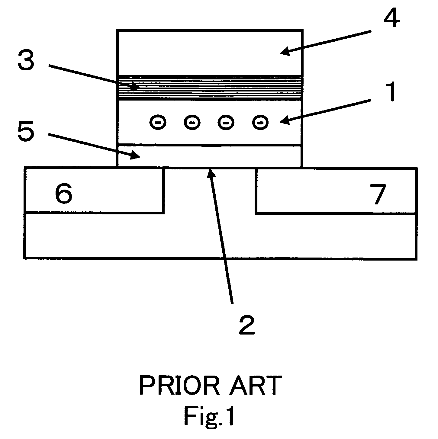
[0034] A nonvolatile memory subjected to the setting method and the screening method of the present invention comprises, similar to a conventional flash memory, a memory cell array having an array of flash memory cells provided of a memory cell structure identical to that shown in FIG. 1 and a memory array control circuit including an address decoder, a voltage generation circuit, a timing control circuit, a sense amplifier and the like for conducting the memory operations (programming, erasing, reading) on each memory cell in the memory cell array. The erasing operation involves applying erasing pulses plural times to a block of the memory cells to be erased so that electrons can be...
PUM
 Abstract
Description
Claims
Application Information
 - R&D
- Intellectual Property
- Life Sciences
- Materials
- Tech Scout
- Unparalleled Data Quality
- Higher Quality Content
- 60% Fewer Hallucinations
Browse by: Latest US Patents, China's latest patents, Technical Efficacy Thesaurus, Application Domain, Technology Topic, Popular Technical Reports.
© 2025 PatSnap. All rights reserved.Legal|Privacy policy|Modern Slavery Act Transparency Statement|Sitemap|About US| Contact US: help@patsnap.com


